Microscopy in the Failure Analysis Workflow
Spatial Resolution
Contrast Mechanisms
Interpretation
Microscopy – What Can and Can’t it Do?
References and Further Reading
Failure analysis, sometimes referred to as failure investigation, aims to determine why a semiconductor device either operates outside its specified parameters (a parametric failure) or fails to perform a required function (a functional failure).
Minimizing unexpected failures is a common goal for all semiconductor manufacturers. However, in sectors such as aerospace and defense, where zero-defect manufacturing is the objective, robust failure analysis becomes an especially critical tool for improving manufacturing processes.1
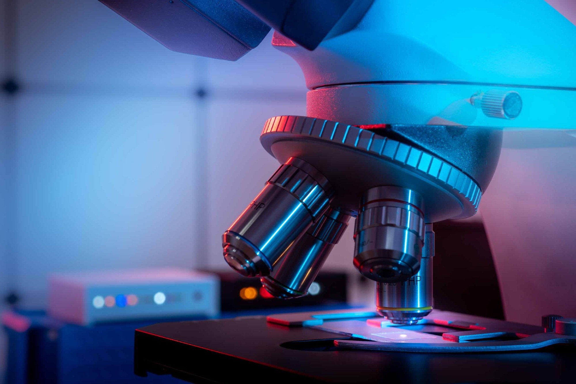
Image Credit: luchschenF/Shutterstock.com
Microscopy in the Failure Analysis Workflow
Microscopy techniques are among the most widely used tools in semiconductor failure analysis because they allow engineers to directly observe defects within a device.
Selecting the most suitable microscopy method, however, is not always straightforward. Several factors must be weighed, including spatial resolution, contrast mechanisms, how easily the results can be interpreted, and whether the technique is destructive or non-destructive.
Save this PDF for later by downloading it here.
A wide range of microscopy techniques are available for failure analysis. Some methods, such as conventional optical microscopy, focus on identifying larger physical defects that may affect device performance, including patterning errors. Others, such as atomic force microscopy (AFM), operate at nanometer-scale resolution and can reveal subtle surface irregularities or defect sites within semiconductor materials that influence device behavior.2,3
Many microscopy techniques are used for direct imaging, including optical, infrared, terahertz, and X-ray microscopy; atomic force microscopy (AFM) and scanning tunnelling microscopy (STM); focused ion beam (FIB) microscopy; and transmission electron microscopy (TEM). Additional specialized methods also play a role. For example, electron beam-induced current (EBIC) and its optical counterpart, optical beam-induced current (OBIC), use microscopy-based approaches to map current flow within a device, offering another way to pinpoint defects.4
With so many microscopy techniques available for failure analysis, how do you decide which is the right choice for failure analysis and root cause identification in semiconductor devices?
Engineers often evaluate several key considerations when making this decision. These include:
- Resolution limits of each technique
- The type of contrast it provides
- How clearly the resulting data can be interpreted
- And whether the method requires destructive sample preparation or allows the device to remain intact.
Spatial Resolution
One of the first factors to consider when selecting a microscopy technique for semiconductor failure analysis is spatial resolution.
Spatial resolution describes the minimum distance between two structures that still allows them to be distinguished as separate objects rather than appearing as a single feature.
In many conventional microscopy approaches, the resolution limit is determined by the wavelength of the illumination source, with shorter wavelengths enabling finer spatial resolution. A number of “super-resolution” microscopy methods have been developed to overcome these limits, although they often require specialized instrumentation and computationally intensive image processing.5
Generally, standard visible-light microscopes achieve spatial resolutions on the order of several hundred nanometers. Using X-ray sources, however, resolutions below 50 nm are possible, and with very short wavelengths, this can extend to below 20 nm.6
Electron microscopy techniques make it considerably easier to reach even higher resolutions. In laboratory environments, sub-10 nm spatial resolution is routinely achievable, which makes these approaches particularly valuable for identifying electrical defects in increasingly small semiconductor devices.7
Contrast Mechanisms
Alongside spatial resolution, the contrast mechanism of a microscopy technique is another important consideration when selecting an approach for semiconductor failure analysis. Contrast determines how defects or structural variations appear in an image and therefore influences how easily they can be identified and interpreted.
Different microscopy techniques also have varying penetration depths, which affects whether frontside or backside regions of a device can be inspected. Optical techniques are particularly useful for identifying surface defects and, when used with polarized light, can also reveal mechanical stresses within materials through birefringence contrast.
Infrared spectroscopy can be used to analyze absorption differences across a device, helping to identify scattering regions associated with defects or variations in defect density. Materials such as silicon are highly transparent to infrared light, allowing IR techniques to image structures beneath silicon layers. This makes infrared methods especially useful for backside inspection in silicon-based devices where frontside access may be restricted.
Scanning electron microscopy (SEM) produces contrast by measuring variations in electrons emitted from the surface of a material. The technique is particularly sensitive to regions containing elements with higher atomic numbers. SEM is also frequently combined with energy-dispersive X-ray spectroscopy (EDS), enabling both defect visualization and elemental analysis. In failure investigations, this combination is often used to identify foreign materials or trace contamination associated with device defects.
Interpretation
Along with spatial resolution and contrast mechanisms, the interpretability of results is another important factor when selecting a microscopy technique for semiconductor failure analysis. Different methods produce different types of images and signals, and the ease with which defects can be recognized or analysed can vary significantly.
Optical microscopy images are generally the most straightforward to interpret. While aberrations and visual artifacts can occur, defects are often visible directly in the image, and even non-specialists can frequently recognize anomalies.
SEM and X-ray microscopy techniques can provide cross-sectional information, but interpreting the resulting images may require careful reconstruction and controlled experimental conditions. Parameters such as detector alignment and imaging configuration can influence the results and thus require careful calibration.
Induced current techniques such as EBIC can also be more complex to perform and interpret. The resulting defect images depend on the initial beam parameters, and charging effects can occur that may complicate the analysis of the measurement. However, EBIC can be particularly valuable for identifying electrically active defects that may not be visible through structural imaging alone.
Transmission electron microscopy (TEM) provides extremely detailed information about device structures. However, sample preparation plays a critical role in obtaining high-quality data.8 While phase contrast imaging can provide information such as device thickness or structural inhomogeneities, interpreting TEM images often requires supporting diffraction data and specialist expertise. For this reason, TEM is often used in later stages of failure analysis when a detailed understanding of nanoscale device structure is required.
Microscopy – What Can and Can’t it Do?
Selecting the most appropriate microscopy technique requires aligning the capabilities of the method with both the size of the device features and the type of defect under investigation. While many microscopy techniques can provide elemental information about defects, achieving both non-destructive inspection and sub-10 nm spatial resolution across an entire device remains challenging with current methods.
Microscopy also has inherent limitations. Spatial imaging alone cannot reveal electrical defects within a device, which means complementary electrical testing methods are often necessary to identify faults related to current flow or circuit behaviour.
Some techniques are better suited to particular failure modes. For example, infrared spectroscopies can help identify thermal issues that arise during device operation. Yet, determining the underlying cause of a failure may still require additional information about device history and manufacturing conditions.
Ultimately, microscopy techniques are highly effective for locating structural defects and visualizing device features. A complete root cause analysis, however, typically requires combining imaging data with electrical measurements, process knowledge, and an understanding of the operational conditions that led to the observed failure.
Microscopy, therefore, plays a central role within the broader failure analysis workflow, helping engineers pinpoint defect locations and mechanisms that can then be linked to manufacturing processes or operational stresses.
References and Further Reading
- Psarommatis, F., May, G., Dreyfus, P. A., & Kiritsis, D. (2020). Zero defect manufacturing: state-of-the-art review, shortcomings and future directions in research. International journal of production research, 58(1), 1-17. DOI:10.1080/00207543.2019.1605228, https://www.tandfonline.com/doi/full/10.1080/00207543.2019.1605228
- Reischl, B., Raiteri, P., Gale, J. D., & Rohl, A. L. (2016). Can point defects in surfaces in solution be atomically resolved by atomic force microscopy?. Physical Review Letters, 117(22), 226101. DOI:10.1103/PhysRevLett.117.226101, https://journals.aps.org/prl/abstract/10.1103/PhysRevLett.117.226101
- Dreyer, C. E., Janotti, A., Lyons, J. L., & Wickramaratne, D. (2024). Defects in semiconductors. Journal of Applied Physics, 136(19). DOI:10.1063/5.0244142, https://pubs.aip.org/aip/jap/article/136/19/190401/3318577/Defects-in-semiconductors
- Dyck, O., Swett, J. L., Evangeli, C., Lupini, A. R., Mol, J., & Jesse, S. (2022). Contrast mechanisms in secondary electron e-beam-induced current (SEEBIC) imaging. Microscopy and Microanalysis, 28(5), 1567-1583. DOI:10.1017/S1431927622000824, https://www.cambridge.org/core/journals/microscopy-and-microanalysis/article/contrast-mechanisms-in-secondary-electron-ebeaminduced-current-seebic-imaging/10.1017/S1431927622000824
- So, S., Kim, M., Lee, D., Nguyen, D. M., & Rho, J. (2018). Overcoming diffraction limit: From microscopy to nanoscopy. Applied Spectroscopy Reviews, 53(2-4), 290-312. DOI:10.1080/05704928.2017.1323309, https://www.tandfonline.com/doi/full/10.1080/05704928.2017.1323309
- Zschech, E., Yun, W., & Schneider, G. (2008). High-resolution X-ray imaging - a powerful nondestructive technique for applications in semiconductor industry. Applied Physics A, 92(3), 423-429. DOI:10.1007/s00339-008-4551-x, https://link.springer.com/article/10.1007/s00339-008-4551-x
- Penczek, P. A. (2010). Resolution measures in molecular electron microscopy. In Methods in enzymology (Vol. 482, pp. 73-100). Academic Press. DOI:10.1016/S0076-6879(10)82003-8, https://www.sciencedirect.com/science/article/pii/S0076687910820038
- Rai, R. S., & Subramanian, S. (2009). Role of transmission electron microscopy in the semiconductor industry for process development and failure analysis. Progress in crystal growth and characterization of materials, 55(3-4), 63-97. DOI:10.1016/j.pcrysgrow.2009.09.002, https://www.sciencedirect.com/science/article/pii/S0960897409000609
Disclaimer: The views expressed here are those of the author expressed in their private capacity and do not necessarily represent the views of AZoM.com Limited T/A AZoNetwork the owner and operator of this website. This disclaimer forms part of the Terms and conditions of use of this website.