Sponsored by AlluxaReviewed by Olivia FrostMay 28 2026
An analytical method for predicting coating-contributed surface error when measurement is limited or inadequate.
Contemporary optical systems demand increasingly tighter tolerances, higher throughput, and greater uniformity over larger apertures. As these performance criteria tighten, so does the need to understand and confidently control the factors that reduce optical wavefront quality.
Among these factors, Transmitted Wavefront Error (TWE) is one of the most crucial yet misunderstood contributors to system-level performance.
TWE quantifies the extent to which an optical element distorts the wavefront of a light wave as it passes through the component. Under ideal conditions, a plane wave would exit a filter or window with no phase-front variation.
In practice, however, optical components introduce non-ideal phase changes or errors arising from several sources, including substrate shape, coating thickness gradients, internal material inhomogeneity, and interactions between multiple surfaces.
These changes/errors can degrade image fidelity, shift focal positions, and introduce aberrations into the optical system.
In some situations, measuring TWE empirically is infeasible. A combination of coating characteristics, wavelength constraints, and instrument limitations may interfere with measurement. Nevertheless, demonstrating compliance remains essential.
To overcome this obstacle, Alluxa’s engineering team has developed an analytical framework for predicting TWE when direct interferometric measurement is impractical or when cost and equipment constraints prohibit complete characterization.
This predictive modeling approach – based on spectral uniformity – is presented as a method for estimating coating-contributed TWE with high confidence when direct measurement is not possible.
TWE Discussion
Transmitted Wavefront Error is the industry-standard metric for quantifying the distortion imparted onto a light wave as it propagates through optical components, such as filters, lenses, and windows. In an ideal optical system, a plane wavefront entering a flat component would exit as an unchanged plane wavefront.
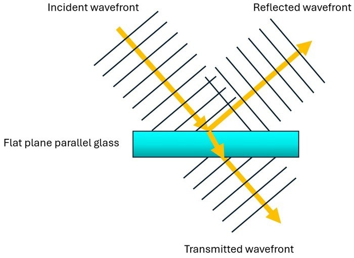
Figure 1a. Light beam wavefront transmitted and reflected by a perfectly flat plane parallel transparent substrate. Image Credit: Alluxa
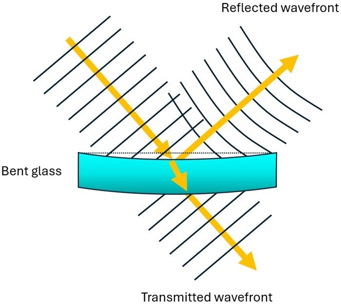
Figure 1b. Light beam wavefront transmitted and reflected by the same glass substrate after bending introduces curvature to the surfaces. Image Credit: Alluxa
In practice, however, nearly all wavefronts deviate from this ideal shape. TWE measures the difference between the emerging wavefront and the ideal reference wavefront.
As a metric, TWE does not usually include all distortions experienced by a wavefront traveling through an optical component.
Piston, tilt, and power (Figure 2) are generally excluded from the final TWE value for the following reasons:
- Piston represents a uniform shift in the phase of the entire wavefront along the propagation axis. While important in some contexts piston can be ignored in most standalone imaging or filtering applications, as it does not alter wavefront shape or image quality. Instead, it merely shifts the absolute phase, which is undetectable to the human eye and standard sensors.
- Tilt occurs when the wavefront arrives at an angle relative to the optical axis. It may result from thickness variation in a component, such as a physical wedge in a substrate, or system misalignment. Tilt does not introduce blur and can often be corrected during system alignment through mirror adjustment or sensor realignment.
- Power is a rotationally symmetric curvature of the wavefront that causes convergence or divergence of a plane wave, effectively acting as a weak lens. Although this aberration can be crucial in fixed-focus systems, it can typically be compensated for in adjustable-focus systems, allowing it to be excluded from the total wavefront distortion.
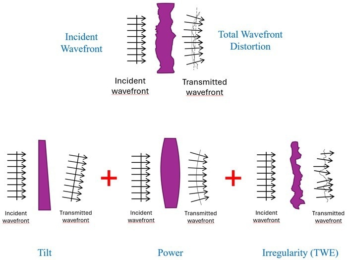
Figure 2. Total wavefront distortion is the sum of piston, tilt, and power components in addition to irregularity. TWE always includes irregularity and sometimes power, but rarely piston or tilt. Image Credit: Alluxa
Although distortions on reflection, known as Reflective Wavefront Error (RWE), may be relevant in some contexts, this discussion focuses on TWE. RWE and TWE are fundamentally different.
For instance, reflection from a slightly bent, plane-parallel substrate (Figure 1b) will exhibit curvature in the reflected wavefront, whereas the transmitted wave remains largely unaffected except for a small tilt.
A common misconception in wavefront error specifications is that surface flatness directly correlates to TWE. In reality, transmitted wavefront error cannot be reliably predicted from the flatness of the two surfaces alone.
Surface geometries of an optical flat may either cancel or compound distortions. When the aspect of one surface matches that of the other, TWE may be minimal (Figure 3b). If they are similar but noncomplementary, TWE can double (Figure 3c).
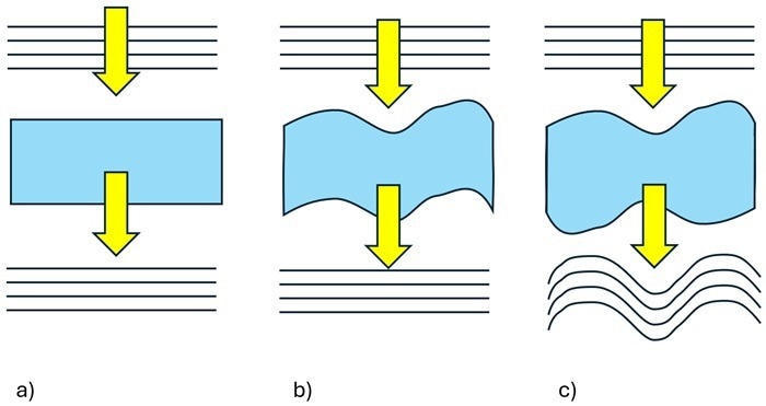
Figure 3. Transmitted wavefront distortion for a) flat substrate, b) substrate non-flat in the same way on both sides, c) substrate with the same non-flat top and bottom surfaces as in b) but with the bottom surface flipped. Image Credit: Alluxa
Calculating TWE from Wavelength Uniformity
TWE is determined solely by variations in the transmitted wavefront, i.e., the relative phase differences across the clear aperture of the optical component. Interferometry is the standard technique for measuring TWE, as it directly maps wavefront phase.
However, this technique is not always practical. Ghost reflections, alignment errors, or opacity of the optic at the interferometer’s source wavelength can all compromise interferometric measurement accuracy.
When interferometry is impractical, TWE can be calculated analytically from wavelength-uniformity measurements across the filter’s working clear aperture. Variations in coating thickness, such as non-uniformity, result in proportional differences in optical phase thickness.
Considering this relationship, wavelength shifts can be directly converted into transmitted wavefront error (Figure 4).
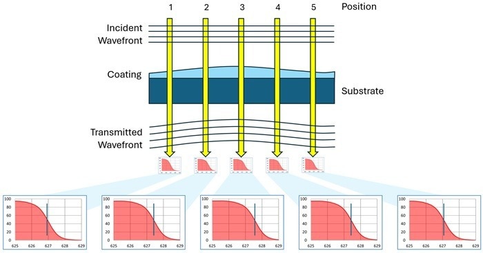
Figure 4. Phase shifts in an incident wavefront after transmission through a filter with variations in coating thickness across the surface. Wavelength dependent features appear at longer wavelengths in areas with thicker coating. Image Credit: Alluxa
This technique relates coating thickness and spectral position to phase variations across the component. The approach relies on several relatively easy-to-satisfy conditions driven by the coating procedure.
First, coating thickness must be the dominant source of wavefront distortion. Wavelength variations across the clear aperture should be driven primarily by coating thickness, with minimal influence from the substrate or other factors. Second, layer thicknesses should scale proportionally across the component. To a first order approximation, all layers in the coating stack should increase or decrease in thickness together.
Third, thickness variations in each layer should be small relative to the layer thickness. This ensures any shift is only a minor phase change and, consequently, can be determined with sufficient accuracy using a first order approximation.
Finally, thickness variations should occur gradually across the surface. This decreases the total number of measurements required to characterize the entire part and allows each measurement to be performed over a reasonable area.
These conditions are commonly met in precision PVD coating procedures such as evaporation and sputtering. During the coating procedure, slight thickness variations inevitably occur due to the variation in deposition thickness within a coating chamber.
As coating thickness increases, spectral characteristics shift to longer wavelengths; as thickness decreases, they shift to shorter wavelengths.
The transmission curve of a thin-film filter is determined by interference between layers and is highly sensitive to layer thickness. Sub-nanometer variations can produce noticeable distortions in the spectral response curve.
To use spectral performance as a measure of TWE, the spectral curve should closely align with the expected theoretical curve, with minimal distortion.
For effective analysis, spectral non-uniformity should manifest as a first order shift in the overall wavelength position; more complex changes in layer-to-layer thickness that impact the final spectral curve would compromise the accuracy of the proposed technique.
In high-layer-count coatings with precise wavelength properties, retention of the spectral curve shape and agreement with the theoretical model provides confidence that thickness variations are small relative to layer thicknesses. Under these conditions, the wavelength shifts can be modeled as a constant percentage change in coating thickness.
After spectral shape integrity has been determined, the procedure for calculating TWE can be summarized as follows: a spectrophotometer or a laser/detector system measures a specific or unique spectral characteristic (e.g., a 50 % edge or peak wavelength) at several locations across the aperture.
These measurements are then plotted as wavelength shifts, as illustrated in Figure 5.
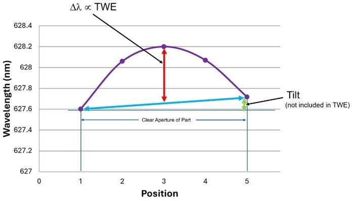
Figure 5. Measured wavelength variation vs. position. A part that has a wavelength dependence, as shown by the purple curve, has a maximum wavelength variation, for TWE purposes, shown by the red arrow. This is less than the maximum change in wavelength across the part, as the linear drift in wavelength, shown by the blue line and green arrow, is ignored. This is because a linear change in wavelength, corresponding to a linear change in thickness or phase, only introduces tilt to the wavefront, and tilt isn’t included as part of the TWE metric. Image Credit: Alluxa
The wavelength shifts are subsequently combined to yield a final maximum shift value for phase or TWE. For a single layer, the phase change is simply the product of refractive index ‘n’ and thickness ‘d’.
For multilayer stacks, calculating the appropriate scale factor requires the use of complex thin-film modeling programs. This is depicted in Figure 6, which presents theoretical transmission and phase for an example case of a 532 nm bandpass filter.
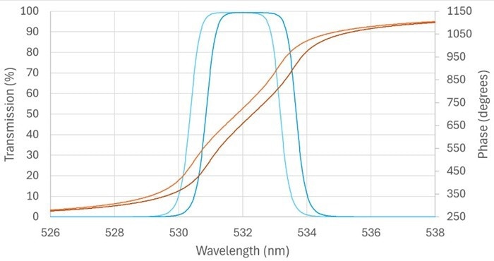
Figure 6. Transmission amplitude and phase for a 532 nm bandpass filter. The two curves are identical filters but with a difference in thickness of 0.1 %. This results in a phase change at 532 nm of about 65 degrees for the wavelength shift of ∼0.49 nm shown. Image Credit: Alluxa
In this example, a 0.1 % thickness variation was modeled using an industry-standard thin-film design program. Introducing this change resulted in a +0.49 nm shift in wavelength, which is clearly visible in both the transmission and phase curves.
The computed phase change provides the scale factor required to relate a given wavelength shift to a given phase change. It should be noted that the phase change, and therefore TWE value, is minimal in wavelength regions of low transmission but is readily determined for wavelengths near the passband.
At the center wavelength of 532 nm, the +0.49 nm shift produces a 65 ° phase change. For this wavelength, the scale factor converting wavelength shift to TWE is calculated as the phase change as a fraction of a full wave (65/360), divided by the wavelength shift producing that phase change (0.49).
This results in a final value of 0.37, which is referred to as the “phase wavelength”. Since TWE is generally expressed in waves, as with flatness, the TWE value would be 1/λ, or 2.7 wavelengths.
In summary, a consistent percentage thickness variation across all layers allows the manufacturer to convert measured spectral shifts into precise, though still approximate, TWE values using the design’s theoretical wavelength sensitivity. As shown in the next section, this approximation is generally conservative.
Validation A: Linear Fit Model
Model validation was performed using a 3-inch diameter substrate with tightly controlled TWE. Prior to coating, this substrate was pre-measured to characterize the surface error.
A custom thin-film bandpass filter was designed with three primary objectives: to optimize transmission at the Zygo Verifire’s 632.8 nm measurement line, to contain an easy-to-reference property such as an edge, and to maximize the phase wavelength factor.
The design was deposited on the pre-characterized substrate, and the resulting device exhibited wavelength dependence as depicted in Figure 7. The goal was to produce measurable non-uniformity across the part.
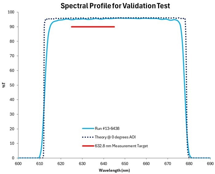
Figure 7. Transmission profile for thin-film validation design, measured on the HELIX spectral analysis instrument with ∼F/10 divergence. Image Credit: Alluxa
Spectral measurements were taken at nine different locations along a line across an approximately 67 mm clear aperture. A spectral non-uniformity of roughly 1.5 % enabled differentiation of the edge properties.
The same part was subsequently measured interferometrically. A 68.5 mm clear aperture measurement allowed direct comparison with the analytical wavelength-shift-derived TWE estimate.
The right side of Figure 8 shows the empirical phase variation across the part measured by the interferometer, presented as both a heat map and a selected cross-section. The left side displays the transmission measurements of the 50 % edge wavelengths of the bandpass, along with a simple linear fit to the data.
The linear fit allows the raw data to be tilt-corrected. These values are subsequently multiplied by the phase wavelength factor, obtained from the design software, to yield the final TWE values.
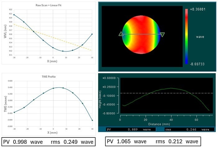
Figure 8. Comparison of TWE values found using analytic TWE calculations compared to values seen using interferometer measurements. Image Credit: Alluxa
The analytically and interferometrically derived TWE results are outlined in the boxes at the bottom of the figure. As shown, the Peak-to-Valley (P-V) values agree within approximately 6 %. The Root Mean Square (RMS) correlation is weaker, which can be attributed to the use of a 4:1 PV-to-RMS conversion ratio, consistent with standard optomechanical practice.1
Validation B: RMSt Grid Method
An alternative approach for calculating TWE uses a grid to analyze the RMS of TWE values across the full surface directly from transmission wavelength variations, rather than relying on a single cross-section.
This technique is generally reserved for higher-value optics, where the additional cost of increased spectral scans can be justified. An order of magnitude more scans (70 versus 9) are necessary to provide adequate point density to analyze TWE over the entire surface.
The following equation is used to calculate TWE:
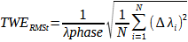
Equation 1. Equation for calculating grid-method TWE.
Where,
- is the phase wavelength of the optical filter stack
- Δλi is the CWL or 50 % edge point deviation from average
- N is the number of scan points
In this example, a grid of spectral scan points was taken across the clear aperture of the component.
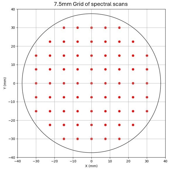
Figure 9. Spectral measurement location over 69 points within the 60 mm clear aperture. Image Credit: Alluxa
The CWL or 50 % edge points for each scan are determined and arranged into a data table depicted here:
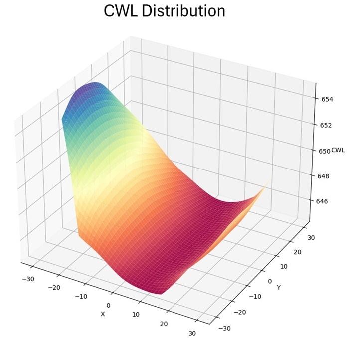
Figure 10. CWL distribution data set. Image Credit: Alluxa
To eliminate piston and tilt for RMSt, an average plane is fitted to the data rather than a line:
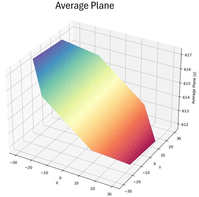
Figure 11. Average plane of CWL data set. Image Credit: Alluxa
The wavelength deviation of each point to its corresponding point on the average plane is plotted:
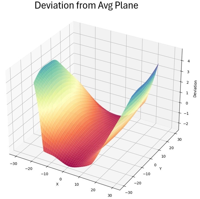
Figure 12. CWL data set manipulated for point-to-point deviation. Image Credit: Alluxa
Referencing Equation 1, the square root of the sum of squares of the deviation is then divided by the phase wavelength to obtain the final value. Figure 13 depicts the result of applying the grid technique to the same part as the linear fit model in Figure 8.
A more in-depth tactic makes this method a more conservative TWE predictor when compared to the empirical interferometric measurement.
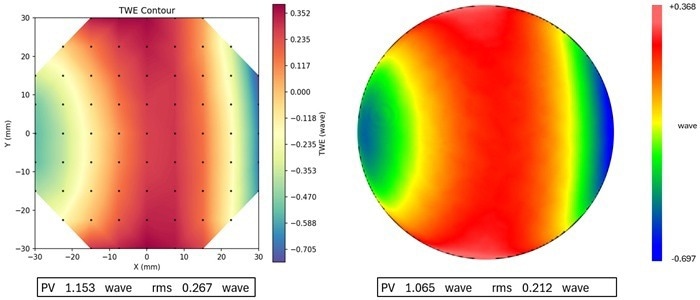
Figure 13. On the left: full 2D analytic TWE values obtained using wavelength scans taken at every grid point location shown by the black points. On the right: a single interferometric 2D scan of the same part. Image Credit: Alluxa
It is worth noting that the grid method RMS reported value employs interpolation and does not fully match the Zygo fit algorithm, since a plane is fitted versus a set of Zernike coefficients.
Application, Next Steps
This analytical TWE instrument is particularly well suited to manufacturing environments, where larger-aperture optics and stringent wavefront specifications frequently strain traditional metrology and procedural controls.
As component sizes grow and clear apertures exceed 50-100 mm, even small coating thickness gradients can introduce system-level aberrations that must be well understood.
By converting routine spectral uniformity measurements into reliable TWE estimates, coating performance is qualified earlier in the manufacturing process, reliance on oversized interferometers is reduced, and the production of windows, large filters, and free-space communication optics can be confidently scaled without introducing metrology bottlenecks.
Looking ahead, applying this technique to real manufacturing parts, such as widefield imaging filters or large-format solar rejection filters for Free Space Optical Communication (FSOC) systems, would allow process engineers to optimize tooling layouts, tuning approaches, and chamber-specific deposition profiles with tighter feedback loops.
In particular, the grid-based RMSt method enables in-depth spatial mapping, supporting root-cause analysis of coating nonuniformity and guiding fixture redesign, rotation schemes, and mask adjustments.
As a next phase, expanding this work into a production-focused “Gen2” study would demonstrate how predictive TWE modeling can reduce scrap rates, enhance coating yield across large components, and provide a scalable qualification path for the high-volume manufacturing of increasingly demanding optical components.
Conclusion
This paper outlines a predictive modeling approach that leverages the fundamental relationship between coating thickness, spectral position, and phase to accurately estimate transmitted wavefront error when interferometric measurements are impractical or unavailable.
Its effectiveness depends on a coating procedure with significantly high deposition precision and repeatability – making it especially well-suited to high-performance platforms such as Alluxa’s SIRRUS™ plasma technology.
Combining spectral uniformity data with linear fits and/or grid-based spatial analysis provides a powerful, physics-driven framework for analyzing and controlling coating-induced wavefront error in production environments.
In turn, this approach enables tighter process tuning, more efficient chamber use, and more dependable qualification of optical filters with rigorous TWE specifications, supporting consistent, scalable manufacturing of high-performance optical components.
References and Further Reading:
- Schwertz, K. and Burge, J. (2012). RMS, P-V, and Slope Specifications. Field Guide to Optomechanical Design and Analysis. (online) DOI: 10.1117/3.934930.ch89. https://www.spiedigitallibrary.org/eBooks/FG/Field-Guide-to-Optomechanical-Design-and-Analysis/RMS-P-V-and-Slope-Specifications/RMS-P-V-and-Slope-Specifications/10.1117/3.934930.ch89.

This information has been sourced, reviewed, and adapted from materials provided by Alluxa.
For more information on this source, please visit Alluxa.