The foundations of the digital world are built on the performances of semiconductor-integrated chips. Semiconductor lithography is the process by which the functional structures within the integrated circuits are patterned.
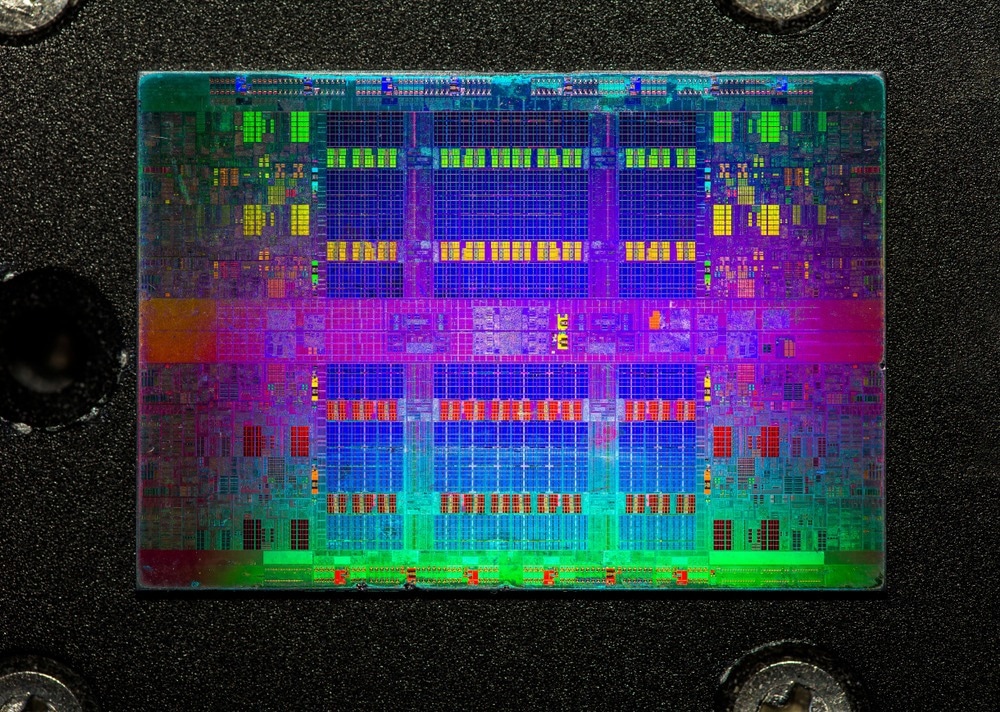
Image Credit: Ersan Uzunoglu/Shutterstock.com
Many devices, including cell phones, automobiles, electrical appliances, and medical equipment, are essential components of daily life and are evolving to become smarter and more functional.
The fundamental building blocks of all digital devices are microchips, primarily made of silicon. Integrated circuits, computer chips, semiconductor chips, and, most commonly, chips are all names for microchips. These chips have to be structured with electrical contacts and circuitry to make them functional and can carry out logic operations and process information. Lithography is the process by which microchips are structured.
Semiconductor Lithography
In essence, a lithography system is a projection system. A "mask" or "reticle"—a template for the design that will be printed—is used to project light through. The proposed pattern on the photoresist material is four times larger on the mask. The system's optics focus the pattern on the mask onto a photosensitive silicon wafer. The system moves the wafer slightly after printing the pattern to create a second copy on the wafer and so on.
Three essential technical components are needed for semiconductor lithography systems, and these affect how well they work.
- The first technology is "the projection lens's resolution capabilities." The more complex a circuit pattern may be when it is optically conveyed, the higher the lens's resolving power. The quality of the lens is usually manufactured through an integrated system of production, starting with the blending of the lens's basic components and continuing with the dissolving, grinding, coating, and assembly.
- "Alignment accuracy" is the second pertinent metric. Photomasks must be changed out dozens of times, and the exposure process must be done many times in order to manufacture a single semiconductor. Thus, it is vitally important that the photoresist wafer is consistently, properly aligned with the photomask. The photomask and silicon wafer are precisely positioned using a number of sensors.
- "Throughput" is the third essential element. Throughput is crucial for the mass production of semiconductors. The quantity of wafers that can be exposed in a given time frame, or throughput, is a measure of productivity. The capability to shift the translational stage where the wafer is fixed at exceptionally high speeds, enabling it to expose the most semiconductors possible on a single wafer and increase throughput, increases the production efficiency.
Semiconductor lithography systems combine the three elements together to produce microchips that handle large volumes of data signals.
Photoresist Material Fabrication
When exposed to light or another source of illumination, the photoresist is triggered to alter its physical characteristics. The photoresist is either formed by dry or wet etching or by turning into volatile chemicals by exposure. Depending on whether the sort of resistance is positive or negative, the pattern formed by the mask either disappears or stays after development. Some of the methods used to treat the photoresist material for semiconductor lithography are highlighted below.
- Etching is a helpful method for selectively removing undesired material to make patterns. Etching mask refers to this technique of material removal.
- During the production of integrated circuits, Many layers consisting of various materials with various properties are deposited on the surface. Physical vapor deposition (PVD) and chemical vapor deposition (CVD) are the two main types of deposition methods used for preparing chip materials.
- The topography of the wafer surface is changed by procedures like etching, deposition, and oxidation, creating a non-planar surface. With the aid of a chemical slurry, chemical mechanical planarization (CMP) is used to flatten the wafer surface.
- The silicon material on the wafer is converted into a silicon dioxide substrate by the enhancement process or stage of oxidation.
- The simplest and most effective method for introducing dopant impurities into crystalline silicon is by ion implantation.
The systems used to manufacture semiconductors by lithography are varied because there is such a wide range of functions provided by microchips. Recent advancements in extreme ultraviolet lithography (EUV) lithography make it possible to pattern the most sophisticated microchips with high-resolution details. The ability of EUV lithography to fit more transistors onto a single chip allows for the mass production of these chips at a reasonable cost. Moreover, they perform better, utilize less energy, and have more brainpower for processing.
Outlook
Chip shortages have captivated the world for the past three years, especially since the Covid outbreak. Yet, there are enough positive factors in the semiconductor market to meet future demand. Automotive, internet of things (IOT), and data center industries are giving the semiconductor industry significant tailwinds.
By increasing silicon printability using numerical computing techniques, computational lithography is also a crucial research topic for the continued growth of semiconductor manufacturing process technology. Artificial Intelligence (AI) is expected to enhance lithography modeling and mask optimization and make an impact on resolution enhancements in the future.
More from AZoOptics: Scientists Publish New Review of Lead-Free Perovskite Based Heterojunction Photodetectors
References and Further Reading
Haoyu Yang and Haoxing Ren. 2023. Enabling Scalable AI Computational Lithography with Physics-Inspired Models. In Proceedings of the 28th Asia and South Pacific Design Automation Conference (ASPDAC '23). Association for Computing Machinery, New York, NY, USA, 715–720. https://doi.org/10.1145/3566097.3568361
Manouras, Theodore, and Panagiotis Argitis. 2020. "High Sensitivity Resists for EUV Lithography: A Review of Material Design Strategies and Performance Results" Nanomaterials 10, no. 8: 1593. https://doi.org/10.3390/nano10081593
Christopher K. Ober, Florian Kafer, Jingyuan Deng, "Review of essential use of fluorochemicals in lithographic patterning and semiconductor processing," J. Micro/Nanopattern. Mats. Metro. 21(1) 010901 (31 March 2022) https://doi.org/10.1117/1.JMM.21.1.010901
Shitnis, S. (30 December 2022) A Perspective on Future of Semiconductor Chip Industry. [Online] Linkedin.com. Available at: https://www.linkedin.com/pulse/perspective-future-semiconductor-chip-industry-shaunak-chitnis/
Nikon. Semiconductor Lithography Systems. [Online] Nikon.com. Available at: https://www.nikon.com/about/technology/product/semiconductor/index.htm
ASML. Lithography – using light to print tiny patterns on silicon – is a fundamental step in mass producing microchips. [Online] ASML.com. Available at: https://www.asml.com/en/technolog
Disclaimer: The views expressed here are those of the author expressed in their private capacity and do not necessarily represent the views of AZoM.com Limited T/A AZoNetwork the owner and operator of this website. This disclaimer forms part of the Terms and conditions of use of this website.