Infrared (IR) imaging is used extensively in modern research and engineering, particularly in semiconductor inspection, materials science, and photonics.
Unlike visible light, infrared radiation can penetrate certain materials and expose subsurface characteristics, making it ideal for non-destructive testing. However, one fundamental shortcoming of conventional IR microscopy is its relatively limited spatial resolution due to the longer wavelengths used.
To overcome this constraint, the LIG Super-resolution Microsphere Amplifying Lens (SMAL) has emerged as an effective optical solution.
The resolving power of standard optical microscopes is considerably improved by SMAL technology, enabling imaging beyond the diffraction limit. The application of this technology in the infrared domain provides new possibilities for high-resolution imaging without the complexities of electron microscopy.
This article provides an overview of the utilization of IR SMAL lenses, with emphasis on their operating principles, experimental technique, and observed performance in practical applications.
Methodology
SMAL Lens Principle
The SMAL lens consists of microspheres with a high refractive index that are positioned close to the sample surface. When illuminated, these microspheres produce a highly restricted electromagnetic field known as a photonic nanojet.
This nanojet interacts with nanoscale characteristics of the sample, capturing high spatial frequency information that would otherwise be lost in traditional far-field imaging.
The microsphere effectively magnifies and projects this near-field information into the far field, allowing it to be detected with a regular optical microscope. This enables the device to bypass the classical diffraction limit and achieve super-resolution imaging.
Infrared Implementation
In the infrared configuration, the SMAL system is modified to work at longer wavelengths (usually in the near-infrared area). This involves:
- Using IR-compatible light sources
- Improving microsphere material and size for IR wavelengths
- Integrating with IR-sensitive detectors and cameras
The experimental setup often includes:
- The LIG Nanowise microscope Nanoro IR or a normal optical microscope with infrared illumination
- Place a SMAL lens directly above or in touch with the sample
- A detecting system that can capture infrared signals
Sample Preparation and Imaging Conditions
Samples examined with IR SMAL lenses usually require minimal pretreatment. Unlike electron microscopy, no conductive coatings or vacuum environments are required. However, the following conditions must be met:
- Sample surface should be relatively smooth
- The microsphere and sample should be separated by only a few micrometers
- Proper alignment and illumination are essential for effective imaging
These conditions ensure that the photonic nanojet and the sample characteristics work together properly
Results and Findings
Resolution Enhancement
One of the most significant findings is that IR SMAL lenses can reach sub-diffraction-limited resolution, even at infrared wavelengths.
While standard IR microscopy has a resolution of several hundred nanometers, SMAL technology can resolve features as small as 150 nm, depending on the setup and conditions.
To demonstrate resolution enhancement, the researchers employ a commercial target sample from Newport (HIGHRES-1) and an NIR light source.
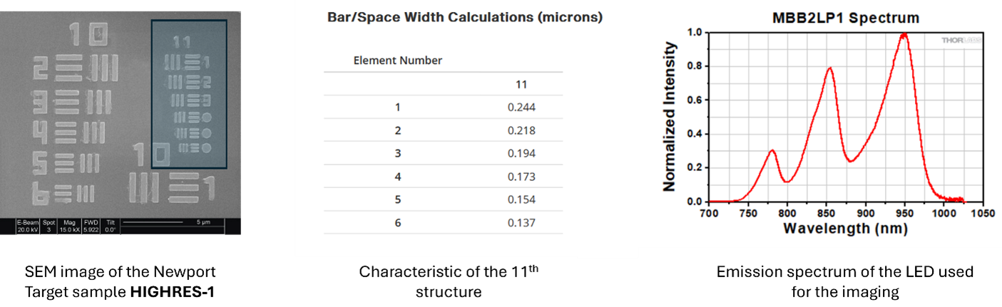
Image Credit: LIG Nanowise
The researchers focus on the 11th pattern, which features particles less than 200 nm in size.
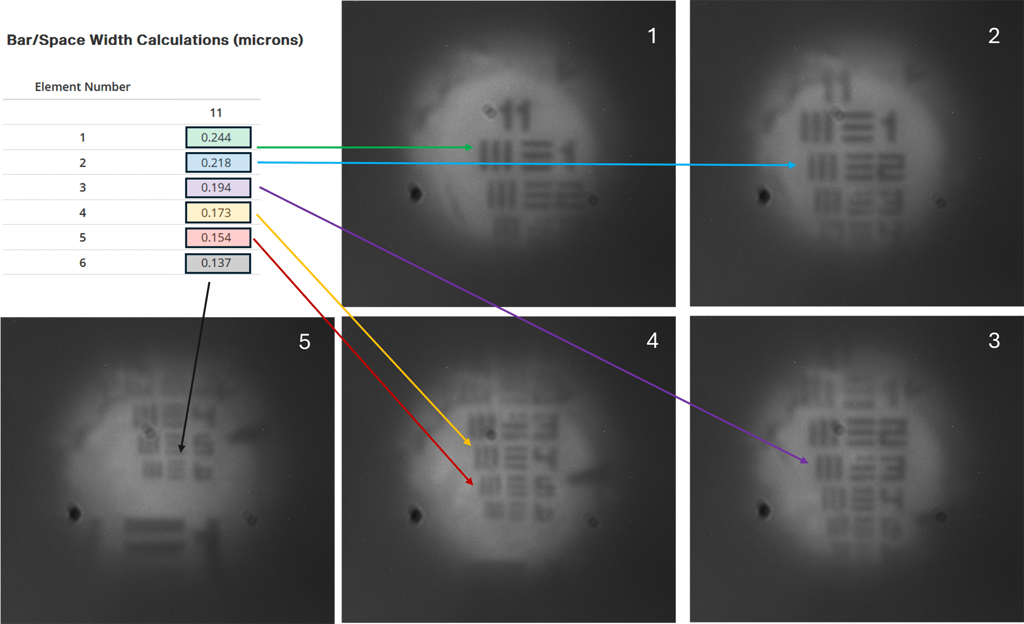
Imaging of 11th pattern of the target sample with IR SMAL. Image Credit: LIG Nanowise
While the smallest pattern, 137, is virtually resolved, the 152 nm pattern is clearly resolved. This is a significant improvement, demonstrating that near-field information may be successfully accessed and used in the IR domain.
Image Quality and Contrast
The usage of SMAL lenses increases image contrast and improves the visibility of nanoscale features. This is especially relevant in infrared imaging, where contrast is typically lower than in visible-light microscopy.
The approach is especially useful for materials with high IR optical sensitivities, allowing for better observation of:
- Subsurface defects
- Layered structures
- Micro- and nanoscale patterns
Real-Time and Non-Destructive Imaging
In practice, the ability to perform real-time imaging without causing damage to the sample is a significant advantage. Unlike SEM and TEM, IR SMAL imaging:
- Operates in ambient conditions
- No need for lengthy sample preparation
- Allows for many observations of the same sample
This makes it ideal for industrial inspection and dynamic studies.
Application Areas
The results show tremendous potential in a variety of fields:
- Semiconductor Inspection: Detection of defects and subsurface features in integrated circuits
- Photonics: Analysis of IR-active devices, including waveguides and optical components
- Materials Science: Investigation of thermal and chemical characteristics at the nanoscale
- Nanotechnology: Characterization of nanostructures beyond traditional IR imaging
Conclusion
LIG Nanowise's infrared version of the SMAL lens marks a significant step forward in optical imaging technology. By bypassing the diffraction limit in the IR spectrum, it allows for high-resolution observation of nanoscale objects that were previously inaccessible using conventional optical approaches.
The combination of super-resolution capability, non-destructive operation, and real-time imaging makes IR SMAL lenses a useful and adaptable instrument for both research and industrial applications.
While several limitations remain, such as the requirement for close contact between the lens and the sample, the overall performance shows great promise for wider implementation.
As infrared imaging becomes more important, SMAL technology is expected to play a critical role in developing nanoscale observation and analysis.

This information has been sourced, reviewed and adapted from materials provided by LIG Nanowise.
For more information on this source, please visit LIG Nanowise.