For many years, optical microscopy has been limited by diffraction limits that have made it challenging to resolve nanoscale structures. Electron microscopy (EM) has been the standard for attaining high resolution, however, it comes with constraints such as complex sample preparation, elevated costs, and a lack of ability to carry out fast, routine scans.
Integrating the SMAL (Super-resolution Microscopy Assisted Lens) into the Nanoro platform resolves these barriers and bridges the gap between optical and electron microscopy. This article presents the performance of the SMAL lens for semiconductor imaging, demonstrating its ability to resolve features down to tens of nanometers with high clarity.
Demonstration on a Semiconductor Sample
To assess the resolving power of the SMAL lens, a semiconductor microchip from an Intel i5 processor was chosen as a test sample. This kind of sample is ideal for resolution demonstrations thanks to its nanoscale features, which are usually identified using a scanning electron microscope (SEM).
- 80 nm features, assessed independently by SEM, were clearly visible with the DRY SMAL lens on the Nanoro M and Nanoro Generation systems alike.
- When used in Blue Mode, the Nanoro Generation produced an even higher level of resolution, making nanoscale details stand out with a high level of sharpness for optical microscopy.
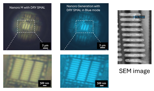
Image Credit: LIG Nanowise
These results underscore how optical microscopy, aided by SMAL technology, can inch toward electron microscopy’s resolution range while maintaining both the ease and flexibility of light-based imaging.
Comparative Imaging Analysis
To explore the benefits stemming from the SMAL lens, a direct comparison was carried out between two imaging setups:
- A scan attained via the Nanoro Generation in Blue Mode with a DRY SMAL lens
- A scan taken using a conventional 100x objective lens
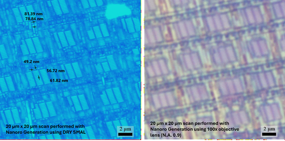
Image Credit: LIG Nanowise
There is a considerable difference in both detail and contrast. While the 100x objective delivers an identifiable image of the microchip surface, the SMAL lens displays nanoscale features with a much higher degree of precision.
Another major upside can be found in the workflow. The Nanoro software makes it possible for users to record high-resolution scans in minutes, greatly reducing the amount of time needed to conduct a nanoscale analysis. Moreover, the software’s integrated measurement tool enables features to be quantified with precision, which ultimately ensures reliability alongside reproducibility in data acquisition.
Concluding Remarks
This demonstration underscores the SMAL lens’s potential to revolutionize the field of optical microscopy. By resolving features as small as 80 nm and more, the technology pushes the boundaries of what can be attained through light-based imaging systems.
When taken with the Nanoro Generation in Blue Mode, the SMAL lens provides:
- SEM-like resolution without the complexity surrounding electron microscopy
- Swift acquisition times, making efficient workflows possible
- Integrated, high-precision measurement tools for robust analysis
Being able to carry out nanoscale imaging quickly and with precision makes this solution especially valuable for semiconductor research, materials science, and advanced manufacturing use cases where speed and resolution are crucial.

This information has been sourced, reviewed and adapted from materials provided by LIG Nanowise.
For more information on this source, please visit LIG Nanowise.