LEDs enable adjustment of the color and intensity of light, and it is therefore possible to use them as efficient and intelligent light sources.
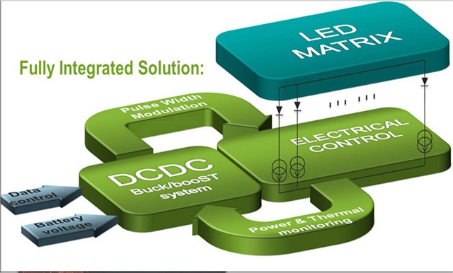 Schematic representation of the optoelectronic device to individually address every pixel of the emitting array. For thermal considerations, the electrical control is kept as thin as possible.
A future smart lighting system based on LEDs could potentially benefit from high-efficiency gallium nitride (GaN) blue-emitting LEDs, integrated electronics, sensors, and microprocessors, and would offer new functionalities and services. Furthermore, monolithic LED arrays (which are characterized by pixelization of the LED emitting area) offer two major innovations: spatial control of light emission, and adjustment of the electrical properties of the source.
The automotive industry uses LED matrices in the fabrication of glare-free vehicle head lamps. Initially, LED package assemblies realized light sources with only a few tens of pixels, but the German project μAFS recently presented a light source with 1000 pixels and 125μm pitch.1 Furthermore, a monolithic LED array can increase the number of pixels to 1,000,000. The main challenges for the source are pixelization of an emitting area with a high active area ratio (the ratio between the emitting and non-emitting areas: the pixel rims), achieving a high-level connection with the electronics, and maintaining the low thermal resistance required to cool the components.
We have demonstrated 300×252 pixels at 10μm pitch using a monolithic LED array.2, 3 We have further developed the GaN etching process to achieve 2.5μm-wide and 7μm-deep trenches. By this means, the active area ratio is more than 96% for a 125μm pitch array. The trenches can be filled with reflective and conductive/dielectric materials, and they act as the electrical spreader, interconnection, and optical isolator.
We eliminated optical crosstalk by etching through the whole GaN structure. Furthermore, the pixels are electrically isolated, allowing serial/parallel reconfiguration for innovative driving solutions (re-arranging the pixels to produce a higher-voltage LED, for example). For a small number of pixels, it is possible to use an electronic interconnection network to address each pixel. For applications requiring more than 1000 pixels (order of magnitude), the driving electronics must be embedded in the LED array submount.
We bonded the arrays using mostly hot processes. LED arrays are grown (by molecular epitaxy) on sapphire and CMOS on silicon, and the thermal expansion coefficients of those two matrices differ by around 5ppm (pixels per million)/K. At 200K, this leads to 1pix per 1000pix. Clearly, HD matrices (1920×1080) would not support this treatment.
To keep the pixel number at an acceptable limit, bonding must be done C2W (chip to wafer). This method is not the ideal choice, as matrices require very precise alignment control. A W2W (wafer-to-wafer) approach is preferable but requires either a low-temperature bonding process or an alternative III-V substrate, such as silicon. To overcome these issues, we investigated various bonding technologies, including bumps, pillars, and microtube bonding with connection densities as fine as 10μm pitch. Microtube technology has successfully enabled microdisplay demonstrations, such as Google Glass.2 Using these approaches, we produced a brightness gain greater than 1000× that of organic LED microdisplays, and reached 10 million Cd (candela)/m2.
Mastering efficient light emission, controlling its spatial location, and embedding electronics in the light source are crucial to next-generation smart lighting systems. The automotive industry has already identified how to achieve simultaneous light and image projection by using low-resolution LED arrays to enable glare-free headlamps. Now other fields—including buildings and street lighting—will benefit from their application.
Our future work will concentrate on further developing monolithic LED array technology to interconnect high-efficiency LEDs in series or parallel strings to operate at higher voltages.