
Grégory Pandraud from Ommatidia LiDAR shares his insights in this AZoOptics Perspectives article on how photonic integrated circuits are revolutionizing sensing and measurement technologies by enabling compact, highly precise, and scalable optical systems. He explores the advantages of PICs for metrology, vibration sensing, and FMCW LiDAR applications, while also examining current challenges and future opportunities for integrated photonics in next-generation instrumentation.
How Photonics Integrated Circuits Are Transforming Sensing and Measurement Capabilities
Photonics has become a cornerstone of modern precision instrumentation. From telecommunications and biomedical imaging to aerospace navigation and industrial automation, optical technologies increasingly enable measurements that exceed the capabilities of traditional electronic systems.
A particularly important development is the emergence of photonic integrated circuits (PICs), which combine multiple optical functions onto a single chip. Much as microelectronics revolutionized computing by integrating transistors into compact integrated circuits, photonic integration is transforming sensing and measurement by miniaturizing complex optical systems while improving performance.
Integrated photonic circuits are becoming important components of next-generation sensors because they offer a unique combination of precision, robustness, scalability, and immunity to electromagnetic interference.
These advantages are particularly valuable in metrology and vibration sensing applications, where measurements often require nanometer-scale precision, operation in harsh environments, and the ability to process large amounts of data in real time.
Recent developments in coherent frequency-modulated continuous-wave (FMCW) LiDAR, laser vibrometry, and distributed sensing illustrate the transformative role of integrated photonics.
Ommatidia LiDAR's multi-channel FMCW platforms provide a compelling example of how photonic integration can enable completely new sensing architectures that simultaneously measure geometry, velocity, vibration, and structural dynamics across multiple points in parallel.
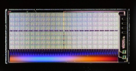
Photonic Integrated Circuit (PIC) designed by Ommatidia LiDAR enabling massively parallel FMCW Laser RADAR. Image credit: Ommatidia
The Metrological and Vibration Measurement Challenge
Modern metrology and vibration measurement systems are increasingly required to deliver high accuracy, high acquisition speed, and robust operation in complex industrial environments.
Traditional electrical sensors such as accelerometers, strain gauges, and displacement probes are still widely used, but these systems often face limitations related to physical contact, wiring complexity, electromagnetic interference, calibration drift, and restricted spatial coverage.
In vibration analysis, contact sensors can alter the dynamics of lightweight structures and require extensive installation effort. In dimensional metrology, conventional point-based measurement approaches may be unable to provide rapid, full-field characterization of large or moving structures.
These challenges are particularly evident in applications such as the structural health monitoring of bridges, modal analysis of industrial machinery, aerospace turbine diagnostics, precision manufacturing, large-scale dimensional inspection, and autonomous vehicle navigation.
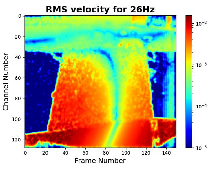
Image Credit: Ommatidia
Modern measurement systems must increasingly combine geometric, kinematic, and dynamic information while maintaining high accuracy and traceability. They must also operate without contact, withstand harsh environments, and acquire large quantities of synchronized data in real time.
Integrated photonics offers a promising path toward meeting these requirements. By combining coherent optical measurement, signal processing, and sensing functions on a single chip, photonic integrated circuits can reduce size, weight, power consumption, and cost while enabling new classes of metrology and vibration measurement instruments with unprecedented performance and scalability.
Integrated Photonic Circuits: A Transformative Technology
PICs are optical systems fabricated on semiconductor substrates that guide, manipulate, and detect light within microscopic waveguide structures.
Much like electronic integrated circuits, PICs combine multiple functions onto a single chip. Depending on the application, a PIC may incorporate lasers, interferometers, couplers, modulators, filters, photodetectors, and signal-processing elements into a compact, robust architecture.
One of the most important capabilities of PICs is their ability to perform ultra-precise phase measurements. Optical wavelengths are extremely short, meaning that interferometric techniques implemented on photonic chips can resolve displacements and vibrations far below a micrometer, often reaching nanometer or even sub-nanometer sensitivity.
In addition, PICs enable sophisticated optical signal processing directly at chip scale, reducing system complexity while improving stability and measurement performance. Their seamless integration with optical fibers further facilitates remote sensing, distributed measurements, and operation in electromagnetically noisy environments.
These capabilities make integrated photonics particularly attractive for a broad range of sensing and metrology applications, including interferometric metrology, laser radar, accelerometers, gyroscopes, displacement sensors, and strain measurement systems.
In many of these applications, photonic integration enables performance levels that are difficult to achieve using conventional bulk-optical or purely electronic approaches.
Several material platforms support photonic integration, with each offering distinct advantages. Silicon photonics benefits from compatibility with CMOS manufacturing and large-scale production. Silicon nitride (SiN) provides exceptionally low optical losses and excellent coherence properties, making it particularly attractive for interferometric sensing and precision metrology.
Indium phosphide (InP) enables the integration of active optical devices such as lasers, modulators, and optical amplifiers. Together, these complementary platforms provide a versatile technological foundation for developing next-generation sensing and measurement systems.
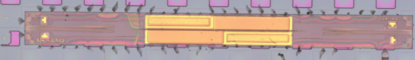
III-V coupons transfer on Si. Image Credit: Ommatidia
Recent advances in coherent FMCW LiDAR demonstrate the power of photonic integration. By integrating dozens of interferometric channels onto a single chip, modern systems can simultaneously acquire distance, velocity, and vibration information across multiple measurement points.
Ommatidia's multi-channel architectures illustrate how integrated photonics enables parallel sensing, replacing conventional scanning approaches with massively parallel optical measurement systems.
Competitive Advantages Over Conventional Technologies
Integrated photonic circuits offer numerous advantages compared with conventional sensing technologies.
The most visible benefit is miniaturization. Functions that previously required multiple optical benches, discrete components, and extensive alignment procedures can now be implemented on a single chip. This dramatically reduces system size and weight while improving reliability.
Environmental robustness is another important advantage. Optical systems are inherently immune to electromagnetic interference, making them ideal for operation near electric motors, power electronics, radar systems, and industrial machinery. Integrated architectures also improve mechanical stability and reduce sensitivity to environmental disturbances.
Improved manufacturability is also significant. Photonic devices can be fabricated using wafer-scale semiconductor processes, enabling repeatable performance and the potential for large-volume production. As photonic foundry ecosystems continue to mature, costs are expected to decrease while device complexity increases.
Integrated photonics also enables entirely new sensing architectures. Multi-channel coherent systems can perform simultaneous ranging, velocimetry, and vibrometry across dozens or even hundreds of points. Parallel acquisition improves measurement speed, eliminates mechanical scanning requirements, and allows real-time visualization of dynamic phenomena such as structural vibration, modal behavior, and wave propagation.
Furthermore, PIC-based systems generally consume less power than equivalent free-space optical assemblies and can be integrated more easily with modern digital electronics, FPGA platforms, and AI-driven processing systems.
Barriers to Adoption
Despite their considerable promise, integrated photonic circuits still face several technical and commercial challenges.
Packaging remains one of the most significant obstacles. Coupling light efficiently between optical fibers, photonic chips, detectors, and electronic circuits requires highly precise assembly techniques. Packaging costs can sometimes exceed the cost of the photonic chip itself.
Thermal management is another challenge. Many photonic devices exhibit temperature-dependent behavior that must be compensated through design, control electronics, or calibration procedures. Maintaining long-term stability under varying environmental conditions remains an active area of research.
Integration with existing electronic systems can also be complex. Successful implementation requires expertise spanning optics, photonics, electronics, software, signal processing, and manufacturing. This multidisciplinary nature can slow adoption and increase development costs.
Finally, while photonic manufacturing has advanced significantly, economies of scale are still developing. Many sensing applications remain relatively specialized, and broader commercialization will require continued investment in standardized design flows, foundry access, and supply chains.
Future Outlook
The future of integrated photonics in metrology and vibration sensing is exceptionally promising. Continued improvements in photonic integration are expected to drive the development of increasingly sophisticated chip-scale measurement systems capable of unprecedented performance.
Digital beamforming, coherent imaging, and massively parallel sensing architectures will likely become standard features of next-generation optical instruments. Artificial intelligence and machine learning will increasingly be integrated with photonic sensing platforms to automate diagnostics, anomaly detection, and predictive maintenance.
Emerging applications include quantum sensing, autonomous transportation, smart manufacturing, structural health monitoring, geophysical monitoring, and space exploration. Integrated photonic LiDAR systems are already being investigated for precision landing and hazard detection during lunar and planetary missions, highlighting the technology's potential beyond terrestrial applications.
As photonic foundries mature and production volumes increase, integrated photonics is expected to follow a trajectory similar to microelectronics, delivering higher performance at lower cost while enabling new classes of instruments.
Conclusion
Integrated photonic circuits are redefining the future of precision measurement. By combining interferometric sensitivity, compact form factors, electromagnetic interference immunity, and scalable manufacturing, PICs provide a powerful platform for next-generation metrology and vibration-sensing systems.
From industrial modal analysis and structural health monitoring to advanced LiDAR and spaceborne sensing, integrated photonics is enabling capabilities that were previously difficult or impossible to achieve.
While challenges remain in packaging, integration, and commercialization, ongoing advances in photonic technologies suggest that IPC-based sensors will play a central role in the evolution of precision instrumentation over the coming decades.
About Ommatidia
Ommatidia reinvents FMCW laser technology for use in 3D velocimetry and micron-level metrology. Inspired by the compound eyes of insects, its innovative LiDAR solutions use an array of miniature optical sensors to capture detailed 3D spatial information with exceptional accuracy and speed. This technology enables real-time depth perception for applications in industrial automation and structural dynamics mapping. By leveraging advanced photonics and signal processing techniques, Ommatidia Laser Radars provide superior performance in terms of resolution, range, and reliability, revolutionizing industrial 3D vibrometry and metrology.