Optical Beam-Induced Current (OBIC) is a laser-based semiconductor analysis technique that generates spatially resolved maps of photocurrent across the surface of an integrated circuit (IC). A focused laser beam scans the surface of a device and generates electron-hole pairs when it strikes a semiconductor region with sufficient energy. This generates a measurable current synchronized with the beam's position, creating a high-resolution map of the device's internal electrical activity.1
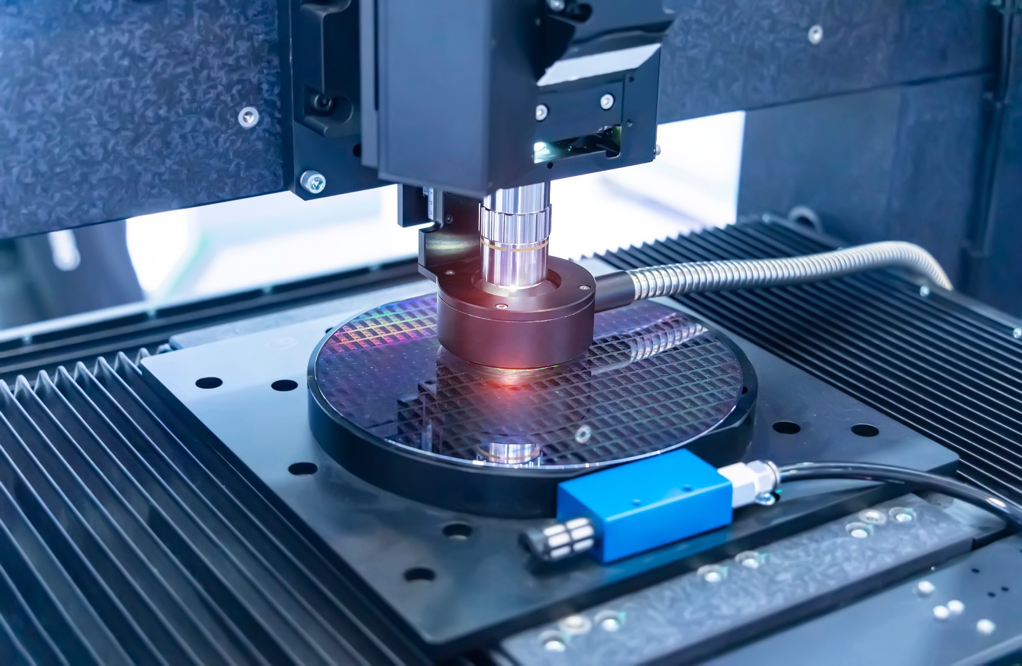 Image Credit: asharkyu/Shutterstock
The Physics Behind Photocurrent Generation
Every semiconductor material has a characteristic bandgap energy, and OBIC exploits this property with precision. Silicon, for example, has a bandgap of approximately 1.12 eV, and researchers commonly use laser wavelengths around 1080 nm (equivalent to roughly 1.15 eV) to generate photocurrent in silicon-based ICs. When the laser targets a defective area, the generated photocurrent differs from that at a healthy site.1,2
In p-n junctions, built-in electric fields separate electron-hole pairs, preventing them from recombining quickly. A well-functioning junction produces a strong photocurrent, while defects weaken this signal. This contrast is exactly what OBIC uses to localize problems.1
Recombination centers at damaged regions act as traps that absorb free carriers before they contribute to the measured current. By analyzing the OBIC signal's strength and spread, researchers can determine the type and density of defects, enabling effective troubleshooting and maintenance of semiconductor devices.1
Sample Preparation and Measurement Setup
One of OBIC's practical advantages in a failure analysis laboratory is its minimal sample preparation. This non-destructive technique doesn't introduce charge into the circuit or damage the device being tested. A typical OBIC setup includes a laser scanning microscope (LSM) and a low-noise current amplifier connected to the device’s power and ground pins.3
OBIC can analyze both the front and back sides of an IC. Back-side analysis is particularly useful for flip-chip devices, where the active components are facing down and hard to access. A near-infrared laser can penetrate the silicon substrate from the back, enabling analysts to explore areas that would normally require destructive methods to access. This flexibility makes OBIC highly practical for modern, densely packaged ICs.3
The resulting OBIC image overlays a photocurrent map with a reflected-light image of the circuit, using two data channels colorized separately for visual clarity. This visual correlation helps analysts quickly identify photocurrent anomalies and isolate failure sites.1,3
Types of Defects OBIC Can Localize
OBIC is a specialized tool designed to detect specific types of defects in ICs. It excels at identifying issues such as damaged p-n junctions, gate-oxide shorts, buried-diffusion regions, and electrostatic discharge (ESD) damage. Each of these defects alters the local photocurrent response in a characteristic manner.1
ESD damage is among the most frequent failure modes in modern ICs, and OBIC detects it by revealing irregularities in the photocurrent distribution near protection structures or junction interfaces.1
Metal-semiconductor interdiffusion, which occurs when metal contact layers migrate into the semiconductor during thermal stress, also creates distinct OBIC signatures that are easily distinguishable from background photocurrent. Additionally, it detects leakage currents from gate oxide damage, mapping these hotspots with sub-micron precision.1
OBIC is also useful in focused ion beam (FIB) milling, where it tracks photocurrent changes as silicon substrates are thinned. The current increases and peaks when the milling reaches the depletion region of a junction, providing a reliable signal to ensure the device remains functional after sample preparation.1
Single-Photon vs. Multiphoton OBIC
Standard OBIC relies on single-photon absorption, where one photon from a continuous-wave laser excites one electron across the bandgap. This mode provides fast scanning speeds and straightforward signal interpretation, and it remains the most common approach in industrial failure analysis labs. The lateral resolution in single-photon OBIC is diffraction-limited, typically in the range of a few hundred nanometers.1
Multiphoton OBIC uses pulsed near-infrared lasers with peak intensities sufficient for two-photon absorption. The main advantage is that the excitation is confined to the beam's focal volume, enabling 3D sectioning of the photocurrent response. As a result, full 3D photocurrent maps of a device can be generated, layer by layer, without physically sectioning the sample.1
Pulsed laser-based single-photon OBIC offers a middle ground, providing time-resolved photocurrent measurements that reveal carrier lifetime and recombination dynamics at defect sites. All three measurement strategies, continuous laser single-photon OBIC, pulsed single-photon OBIC, and multiphoton OBIC, address different analytical questions and are selected based on the specific defect type and device architecture being investigated.1
OBIC Versus EBIC in Failure Analysis
Electron Beam-Induced Current (EBIC) is OBIC's closest competitor in the defect localization space. Both techniques measure the current generated when a semiconductor is excited, but they differ significantly in the nature of their probes.4
EBIC uses an electron beam in a scanning electron microscope (SEM), which requires a vacuum and can affect the device being tested. In contrast, OBIC operates under ambient conditions, making it easier to use. Since OBIC does not introduce additional charge carriers, it avoids problems associated with altered electrical states. This aspect is very important for thin gate oxides, where even minor changes can affect performance.3,4
EBIC retains advantages in spatial resolution, since electron beams can be focused more tightly than diffraction-limited laser spots. However, OBIC's non-destructive nature, ambient operating conditions, and compatibility with back-side analysis make it the preferred technique for many practical failure analysis workflows in semiconductor manufacturing.1,3
Current Directions and Future Potential
Advances in laser technology and detector sensitivity are broadening OBIC's analytical reach. With improved numerical-aperture objectives and shorter laser wavelengths, OBIC can achieve spatial resolutions below 300 nm, narrowing the gap with electron-beam methods. Researchers are also integrating OBIC with confocal reflectance imaging and other techniques to capture more information in a single scan.1
The growing complexity of 3D IC architectures, where multiple active layers are stacked vertically, places new demands on non-destructive defect localization methods. Multiphoton OBIC is positioned to meet this demand directly, as it can effectively map photocurrents in stacked layers without altering the samples. This capability reduces analysis time and minimizes potential errors.1
Saving this for later? Download a PDF here.
As IC nodes shrink below 3 nm, the need for precise defect localization increases. This requires ultra-low-noise amplification and stable beams. The technique's ongoing development in these areas ensures it will remain a core method in semiconductor failure analysis for the foreseeable future.5
References and Further Reading
- Zhuo, G. Y. et al. (2022). An insight into optical beam induced current microscopy: Concepts and applications. Microscopy Research and Technique, 85(11), 3495-3513. DOI:10.1002/jemt.24212. https://analyticalsciencejournals.onlinelibrary.wiley.com/doi/10.1002/jemt.24212
- Optical Beam Induced Current (OBIC). Watson Analytical LLC. https://www.watsonanalytical.com/service/optical-beam-induced-current
- Optical Beam Induced Current (OBIC). MU Analysis. https://muanalysis.com/optical-beam-induced-current
- EBIC/EBAC Semiconductor Failure Analysis. WinTech Nano. https://en.wintech-nano.com/ebic-ebac/
- Buragohain, A. et al. (2024). Facile Construction of a Laser Scanning Optical Beam Induced Current Microscope. IEEE Photonics Journal, Vol. 16, No. 1. DOI:10.1109/JPHOT.2024.3349930. https://ieeexplore.ieee.org/stamp/stamp.jsp?arnumber=10380660
Disclaimer: The views expressed here are those of the author expressed in their private capacity and do not necessarily represent the views of AZoM.com Limited T/A AZoNetwork the owner and operator of this website. This disclaimer forms part of the Terms and conditions of use of this website.