Semiconductor manufacturing at nanoscale technology nodes requires precise defect inspection to ensure optimal yield and device reliability. Conventional optical inspection faces challenges in detecting smaller and more complex defects. Electron beam (e-beam) inspection has emerged as a high-resolution alternative, allowing superior defect sensitivity at the nanoscale. This article compares the utility of both inspection modalities.1-4
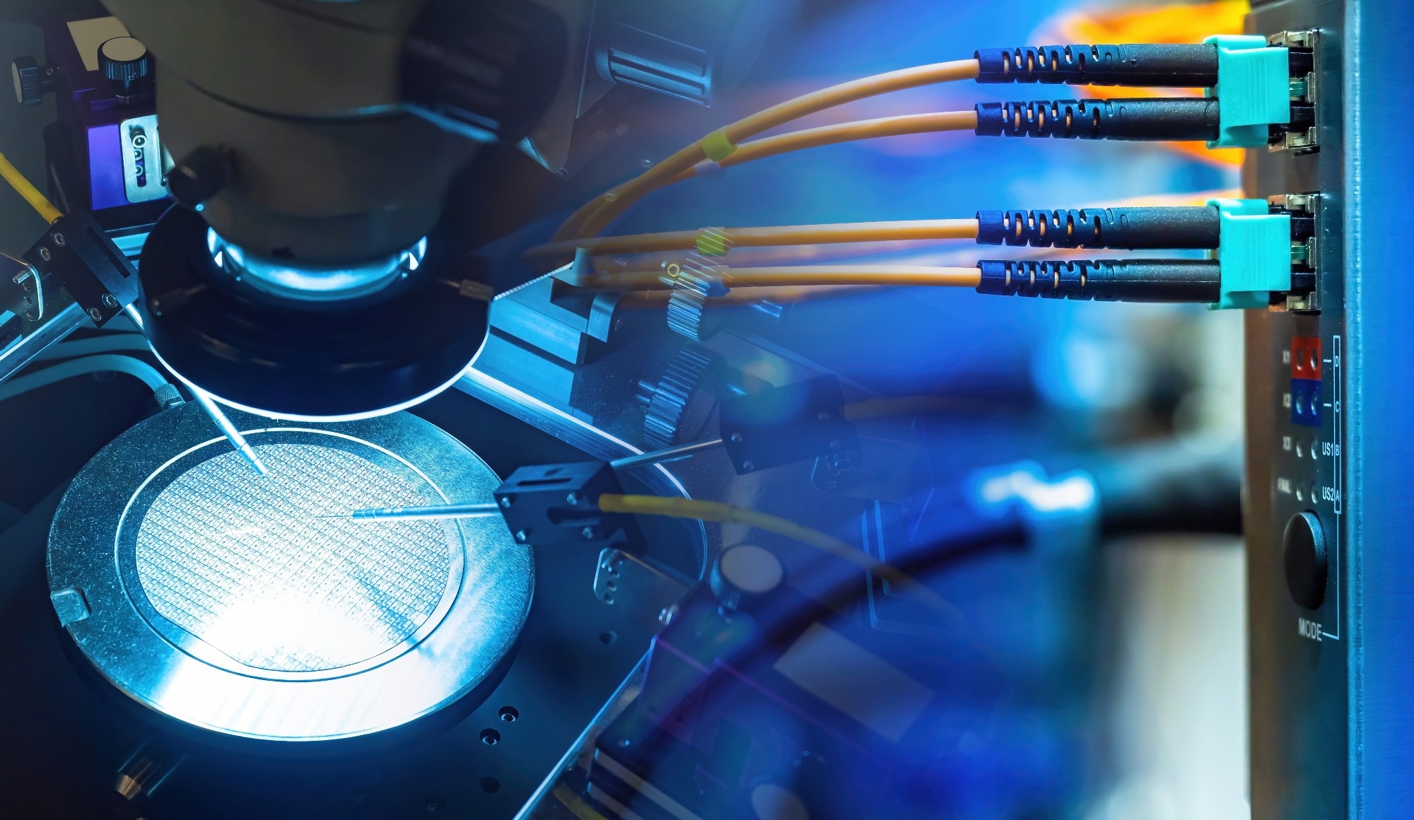 Image Credit: FOTOGRIN/Shutterstock
The Need for Advanced Inspection
The rising demand for smart devices, electronic devices, and the Internet of Things is reducing the critical dimensions and increasing the circuit complexity of integrated circuits (ICs).1,2
The mainstreaming of sub-10 nm high-volume manufacturing has increased the importance of accurately detecting more complex, smaller defects that impact manufacturing cost and yield. Recently, Taiwan Semiconductor Manufacturing Company and its Research Alliance partners announced a breakthrough in 3 nm technology. 1-3
Ever-decreasing sizes of spaces and features in patterns have created challenges in inspecting wafer defects. The number of inspection steps increases with the number of patterning steps, as triple, double, or quadruple patterning in ultraviolet lithography is commonly used now.1,2
An increasing number of inspection steps reduces throughput and increases the risk of device failures, as missed defect-detection events are transferred to the end process. The inspection system for detecting wafer defects identifies pattern and physical defects on wafers and obtains their position coordinates.1,2
Defects are classified as systematic defects and random defects. Systematic defects are caused by deviations in the mask and exposure process. These defects occur in a similar position on the circuit pattern of all projected dies. Random defects are attributed to particles that attach to the wafer surface; thus, their positions cannot be predicted.1,2
Optical Inspection
Optical inspection is one of the most direct approaches for inspecting defects on a patterned wafer. Optical far-field inspection/brightfield microscopy has low-dose exposure and a large field of view. In the fab, brightfield inspection identifies critical defects. Light reflected from a defect is collected by brightfield, and the defect appears dark against a white background.1,2
Chipmakers want higher throughput and improved signal-to-noise ratio in optical inspection. While optical is faster, it is being stretched to the limit at advanced nodes. At the sub-10 nm design node, extreme ultraviolet (EUV) wavelength utilized in wafer inspection is reaching its limits in detecting defects.1
Super-resolution deep ultraviolet (SR-DUV) wavelength bands can capture yield-critical defects at 10 nm design nodes and beyond, extending the longevity of optical inspection tools.1
While brightfield microscopy suffers from the Rayleigh limit, the signal-to-noise ratio and contrast are the key to defect inspection. A d6/λ4 scaling of the detectable far-field signal is certain for a scatter with size d in Rayleigh scattering.2
Noises from the sample side (such as line-width roughness and line-edge roughness of the background nanopattern) and the imaging component side (such as mechanical instability, lens defects, and shot and readout noise in the camera sensors) degrade image contrast and overwhelm the scattering signal from nanoscale defects.2
E-beam Inspection
E-beam inspection locates and characterizes tiny defects with feature sizes down to 1 nm. This tool localizes “defects”/local abnormalities on the semiconductor wafer surface. E-beam inspection tools are utilized in two modes.1,2
In the first mode, the e-beam obtains images of sufficiently large areas to capture a physical abnormality or defect. In this physical defect inspection, the defect appears in the imaged area and is visible in the detector image.1
The second mode involves voltage-contrast inspection, in which changes in the wafer surface potential are detected. Such changes can occur due to a physical defect, such as an electrical defect that causes higher electrical leakage, or due to a particle. In both cases, voltage change at the particular location on the wafer is sensed by the e-beam inspection tool as the proxy for the defect itself.1
A traditional e-beam inspection uses an electron beam to irradiate the target region, which causes the emission of secondary electrons. The intensity of the secondary electron emissions is measured by a secondary electron detector along the scan path of the e-beam.1
While the region is scanned, surface voltages induced by the electron beam vary across the scanned region due to differential charge accumulation on the irradiated features.1
Comparison of Optical and E-beam Inspection Modalities
Optical and e-beam inspection methods have distinct advantages and limitations in defect detection. Due to the physical resolution limits of optical techniques, detecting nanoscale defects in shrinking device geometries has become increasingly challenging.1,2
Thus, e-beam inspection has gained importance, particularly for sub-10 nm technology nodes, due to its superior resolution and ability to detect small and buried defects that optical tools miss. E-beam inspection can realize resolutions approaching 1 nm and provide detailed defect characterization, making it suitable for advanced process development and defect analysis.1,2
However, e-beam inspection is limited by low throughput due to a small field of view and slow scanning speed. Although multi-column e-beam systems have been developed to improve inspection speed, challenges such as image stitching and alignment accuracy remain. Thus, e-beam inspection is still considerably slower than optical inspection.1,2
Saving this for later? Download a PDF here.
Optical far-field inspection continues to dominate wafer inspection in high-volume semiconductor manufacturing due to its large-area coverage, high speed, and suitability for in-line production.1,2
Yet, its moderate resolution restricts its ability to detect the smallest defects. In contrast, e-beam inspection offers higher resolution and identifes both physical and electrical defects but is used for advanced defect analysis and research applications.1,2
Overall, optical and e-beam inspection serve as complementary technologies: optical inspection provides efficient, high-throughput monitoring, while e-beam inspection delivers detailed nanoscale defect characterization, making both crucial for modern semiconductor manufacturing.1,2
Inspection Modalities for Advanced Nodes
A balanced integration of optical and e-beam inspection remains essential as semiconductor technology advances toward smaller nodes. Optical inspection continues to provide high-throughput wafer monitoring, while e-beam inspection enables precise nanoscale defect characterization.
New developments, such as the 2024 SEMI Advanced Semiconductor Manufacturing Conference (ASMC) study on critical defect detection at the 3nm technology node using DUV optical inspection with artificial intelligence-based algorithms, demonstrate the potential to enhance optical capabilities.4 Future inspection strategies will depend on combining advanced imaging, AI-driven analysis, and complementary modalities to improve yield and reliability.
References and Further Readng
- Oberai, A., & Yuan, J. S. (2017). Smart E-Beam for Defect Identification & Analysis in the Nanoscale Technology Nodes: Technical Perspectives. Electronics, 6(4), 87. DOI: 10.3390/electronics6040087, https://www.mdpi.com/2079-9292/6/4/87
- Zhu, J. et al. (2022). Optical wafer defect inspection at the 10 nm technology node and beyond. International Journal of Extreme Manufacturing, 4(3), 032001. DOI 10.1088/2631-7990/ac64d7, https://iopscience.iop.org/article/10.1088/2631-7990/ac64d7
- Kundaliya, D. (2020) TSMC to begin 3nm mass production in 2021, report [Online] Available at https://www.computing.co.uk/news/4017969/tsmc-begin-3nm-mass-production-2021-report (Accessed on 16 July 2026)
- Chiu, S. C. et al. (2024). Critical Defect Detection at 3nm Technology Node: Enhanced Detection Using DUV Optical Inspection Technology With AI-Based Algorithm. 2024 35th Annual SEMI Advanced Semiconductor Manufacturing Conference (ASMC), 1-5. DOI: 10.1109/ASMC61125.2024.10545367, https://ieeexplore.ieee.org/abstract/document/10545367
Disclaimer: The views expressed here are those of the author expressed in their private capacity and do not necessarily represent the views of AZoM.com Limited T/A AZoNetwork the owner and operator of this website. This disclaimer forms part of the Terms and conditions of use of this website.