A Van der Waals (vdW) Integration Strategy Decouples Crystal Growth from Silicon and Silicon Nitride Chip Fabrication, Preserving Material Quality While Enabling Electro-Optic Modulation, Magneto-Optic Nonreciprocity, Multi-Material Photodetection and Vertically Stacked Optical Functions.
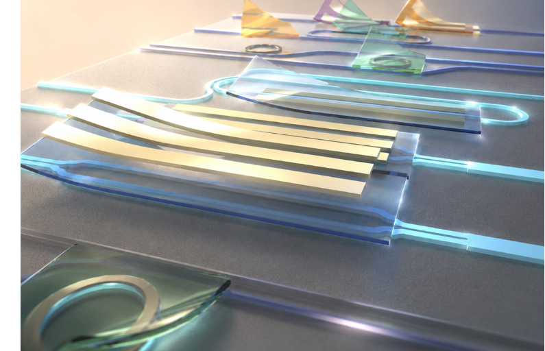 Heterogeneous photonic circuit enabled by van der Waals integration. Image Credit: Yuan Meng, Sang-Hoon Bae.
Overcoming Material Incompatibility in Heterogeneous Photonics
Photonic integrated circuits use light for high-bandwidth, low-loss communications, sensing, computing and quantum technologies. Silicon (Si) and silicon nitride (SiN) are mature waveguide platforms but lack several essential functions. Efficient electro-optic modulation, optical isolation and detection over widely separated wavelengths require additional crystals. Integrating these crystals without degrading their properties remains difficult. In direct heteroepitaxy, lattice mismatch or incompatible processing between the functional layer and chip can generate defects, strain and crystallographic disorder, weakening electro-optic, magneto-optic and optoelectronic performance.
Researchers from Washington University in St. Louis, EPFL, MIT and collaborating institutions report in Nature an alternative sequence. A material is grown on a suitable parent substrate, released as a freestanding single-crystalline 3D nanomembrane, and transferred to a prefabricated Si or SiN circuit. Since the membrane need not inherit the chip lattice, crystal growth and device fabrication can be optimized independently.
Assembling Functional 3D Crystals on Photonic Circuits
The membranes were produced by epitaxial lift-off, which removes a sacrificial layer, or by 2D-material-assisted layer transfer, including remote epitaxy. The material library includes barium titanate (BTO), cobalt ferrite (CFO), yttrium iron garnet (YIG), gallium arsenide (GaAs) and gallium nitride (GaN).
Freestanding membranes can be oriented, stitched laterally across separate circuit regions, or stacked into artificial heterostructures. The method extends vdW integration beyond layered 2D materials, enabling non-layered 3D crystals to be assembled on a finished chip without lattice-matched growth.
Engineering BTO for a Giant Electro-Optic Response
In BTO-on-Si Mach-Zehnder modulators, performance depends on crystallinity, ferroelectric domains and crystal-axis alignment. To access BTO's large Pockels response, predominantly a-axis-domain membranes were rotated by about 45° relative to the waveguide, maximizing the effective coefficient.
At 1 kHz and 1,550 nm, a modulator achieved a half-wave voltage-length product (VπL) of approximately 0.29 V·cm. Its effective in-plane Pockels coefficient was about 950 pm/V, corresponding to an estimated r42 above 1,290 pm/V - roughly 40 times the relevant coefficient of established lithium-niobate or lithium-tantalate platforms. This confirms that transfer preserved the single-crystalline quality and orientation-dependent BTO response.
Efficiency and speed were demonstrated in separate designs. A travelling-wave modulator using 45-nm BTO, a 250-nm SiO2 spacer and matched electrodes reached a 3-dB bandwidth above 23 GHz, VπL of approximately 1.4 V·cm at 2 MHz and an effective Pockels coefficient near 880 pm/V. The two devices therefore address different efficiency-bandwidth regimes.
Magneto-Optics Photodetection and Vertical Nanomembrane Stacking
Single-crystalline CFO on Si microrings produced nonreciprocal clockwise-counterclockwise splitting with more than 18 dB extinction under a permanent magnetic field. The extracted Faraday rotation coefficient was approximately 33,800°/cm - about 100 times that of YIG and 10 times that of cerium-substituted YIG in the paper's comparison. Because CFO is hard magnetic, nonreciprocal operation can persist after magnetization without a continuously applied magnet.
Laterally integrated GaAs and GaN nanomembranes provided material-selective detection on one SiN circuit. The proof-of-concept devices achieved 0.30 A/W at 780 nm and 0.16 A/W at 520 nm with GaAs, and 17 mA/W at 405 nm with GaN, spanning discrete near-ultraviolet to near-infrared wavelengths.
Vertically stacked CFO and BTO membranes, separated by SiO2, combined electrical tuning and magnetic nonreciprocity on one Si microring. The device produced an approximately 5-pm nonreciprocal shift and more than 13 dB extinction, illustrating how artificial heterostructures can unite single-crystalline functions that conventional heteroepitaxy cannot readily combine.
Outlook and Remaining Challenges
The platform preserves near-bulk crystal quality while making crystal orientation, lateral placement and vertical sequence independent design variables. Demonstrations ranged from centimeter-scale pieces to a one-inch-diameter BTO membrane, with smooth surfaces, sharp interfaces and robust bonding after thermal treatment.
The platform supports multifunctional heterogeneous photonics and studies of coupled ferroelectric, magnetic and semiconductor crystals. It is not yet a foundry-qualified process: wafer-scale placement, alignment yield, interface uniformity, automation, packaging and long-term reliability require further development. Nevertheless, optimized epitaxy followed by physical assembly enables material combinations previously excluded by lattice and process incompatibility.