Anti-reflection (AR) coatings are crucial elements in contemporary optical and imaging systems, as they reduce undesired Fresnel reflections at air-glass interfaces to prevent internal flare and ghosting from compromising image contrast while maximizing system light throughput.
A wide variety of instruments and spectrophotometers excel at quickly and easily measuring the performance of these coatings on an optical flat sample at discrete incidence angles.
However, this macroscale instrumentation is not appropriate for measuring samples with realistic curvature, as curvature in the measurement region will destroy the phase coherence necessary to resolve thin-film interference.
Microspectrophotometers (MSPs) address these challenges by restricting the sampling region to 20 µm or less. This allows the curved surfaces to be locally planar for the measurement, with radii of curvature as small as 200 µm.
In addition, by using aperture-defined confocal imaging and Fourier-plane angular weighting, CRAIC microspectrophotometers provide accurate characterization of AR coatings on microlenses without spectral contamination from back-surface reflections.
Background
AR coatings are formed by sub-micron dielectric stacks that produce precise constructive and destructive interference patterns to attain minimum reflectance at certain wavelengths.
Characterization of these coatings requires maintaining strict local wavefront flatness of at least λ/2 over the illuminated spot to ensure maximum coating performance accuracy; If this limit is exceeded, phase incoherence is introduced throughout the measurement region, potentially washing out the spectral interference fringes.
To treat the surface as locally planar, the measurement region must be substantially smaller than the radius of curvature (R). For a given measurement region, the maximum curvature can be defined by observing the optical sagitta s (or sag), which defines the curvature or bow for a spherical surface across a given region, as shown:
s ≈ r2/2R
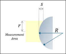
Figure 1. Diagram of Optical Sagitta, s, where r is the radius of the sample measurement area and R is the radius of curvature of the surface. Image Credit: CRAIC Technologies
Assuming work in the visible (i.e., 400–700 nm) and a deformation tolerance of λ/2, for an average wavelength of 550 nm (or 0.550 µm), the sag s value is 225 µm.
Solving for R using a 1 cm sampling region versus a 20 µm sampling region produces radii of curvature of 45.4 m and 182 µm, respectively. The most common lenses typically possess curvature dimensions between 500 µm and 50 mm, making a microscale sampling region on the order of tens of microns crucial.
In addition to restricting the lateral sampling region, two key optical variables must be managed when measuring AR coatings on microlenses.
- Managing depth of field (DoF) to isolate front-surface coatings from back-surface reflections
- Accounting for objective numerical aperture (NA) and angular weighting impacts on these interference patterns
Depth of Field and the Back-Surface Reflection
When measuring low-reflectance AR coatings, a secondary Fresnel reflection from the uncoated back surface of a thin substrate can readily overpower the signal from the front coating.
Moreover, unlike isolated point objects described by conventional microscopy DoF formulas, continuous planar back surfaces reflect light into the optical train across a wide axial range.
When using conventional widefield Köhler illumination, a flat mirror surface that is 250 µm out of focus still returns almost 10% of the maximum intensity back into the collection light path, resulting in severe distortion of the AR coating’s spectral response.
However, closing the microscope field stop creates a dual-aperture confocal spatial filter within the microscope, significantly sharpening the MSP’s depth-of-field response.
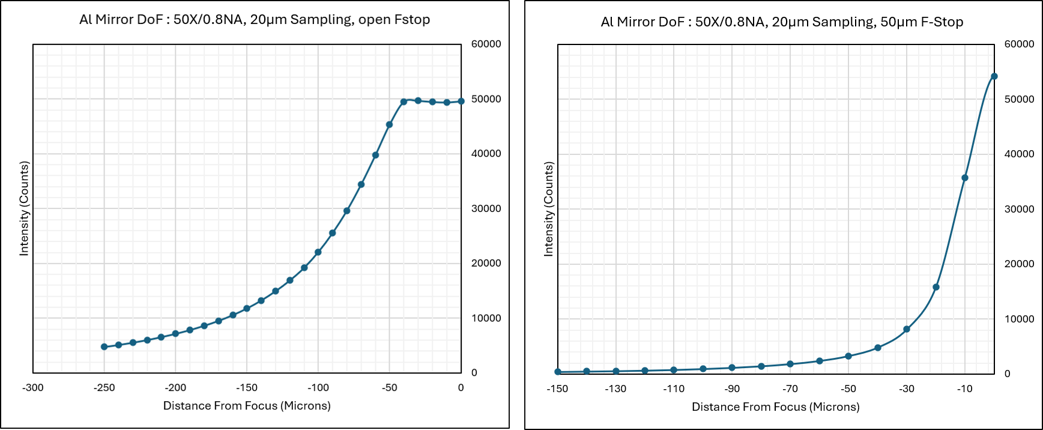
Figure 2. Left is the signal from a wide-field microscopy setup with significant out-of-plane contributions extending to several hundred microns. Right is with a confocal detection setup showing how the signal from out-of-focus planes falls off sharply, enabling clean isolation of front-surface coatings on air-spaced substrates as thin as 150 µm. Image Credit: CRAIC Technologies
This dual conjugate aperture configuration enables measurements of samples down to 150 µm within the visible spectrum, with no contribution from surfaces at that distance or farther, assuming the medium's refractive index matches that of air.
When measuring transparent optical coatings, the light cone propagates through a medium with refractive index n > 1. Refraction compresses the internal ray angles while extending the optical path length relative to measurements performed in air.
For standard optical glasses (n ∼1.2–1.5), the effective axial exclusion zone expands by 20% to 50%, establishing a practical minimum lens thickness threshold of 225 µm. For high-index semiconductors such as Silicon (n ∼3.5 in the NIR), this broadening is significantly larger and must be explicitly accounted for during aperture selection and sample preparation.
Angle of Incidence Impacts on Interference Patterns
Macroscale instruments evaluate these thin films using collimated light at a single well-defined angle of incidence, θ. Conversely, a microscope objective focuses light across a continuous range of angles spanning from θ = 0 (perpendicular to the surface) up to the maximum permitted by the objective numerical aperture (NA), θ = asin(NA).
NA = n * sin θ
By employing thin-film modeling software that uses the real and imaginary refractive indices of the involved materials (n and k, respectively), the reflectance spectrum change can be calculated with increasing incidence angles, as depicted in Figure 3.
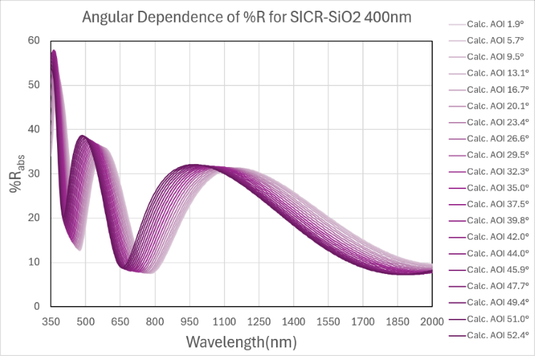
Figure 3. Modeled Reflectance spectra for 100 nm of SiO2 on a polycrystalline silicon wafer, demonstrating the two key changes of dampened interference patterns and blue-shifted spectra that are observable with increasing incidence angles (light to dark purple). Image Credit: CRAIC Technologies
This model demonstrates that increasing the incidence angle has two different effects on the spectrum. First, it blueshifts the observed maxima and minima. Second, it dampens the interference pattern, decreasing the contrast between maxima and minima.
For accurate modeling or quantification of AR coating performance under an MSP, the raw reflectance spectrum must be treated as a composite sum of all incident angles within the objective's illumination cone.
r = f * n * sin θ
dA = 2 * π * r * dr
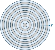
Figure 4. Diagram of the Fourier plane illustrating how higher incidence angles correspond to larger differential areas. Image Credit: CRAIC Technologies
Located at the back focal plane of an objective, the Fourier plane provides the best method for considering and measuring the incidence angles. If the objective meets the Abbe Sine Condition, which is standard for modern Köhler illumination microscopes, then the radial distance r from the optical axis is directly proportional to sin(θ).
Since the geometric area of an annular ring in the Fourier plane scales with its radius, higher incident angles deliver a larger proportion of the total energy to the focused spot compared to rays close to the optical axis.
Calculating the light ratio at angles from θ = 0 to the maximum of θ = asin(NA) yields a weighting distribution by incidence angle solely based on the differential area in the Fourier plane. This is described assuming either an even intensity distribution in the Fourier plane1 or a Gaussian intensity distribution over angles.2,3
Integrating this angular weighting into CRAIC’s FilmPro modeling software enables users to generate anticipated spectral profiles corrected for the microscope objective’s incident-light profile, ensuring accurate extraction of coating thickness from the observed interference patterns.
Measurement Results
The spectrum is always in relative reflectance when measuring thin films on the MSP. More information on this topic is available in CRAIC Technologies’ Applications Note on Reflectance Measurements with the Microspectrophotometer. For the spectra displayed here, the coating thickness results for Silicon Dioxide (SiO2) on Silicon were previously measured using an ellipsometer.
The MSP measurements were gathered on a 2030PV Pro microspectrophotometer using a 50X magnification EC Epiplan Neofluar objective with 0.8 Numerical Aperture. To maximize confocal performance, the instrument was configured using a 20-micron sampling aperture and a 50-micron field-stop diameter.
The uncoated region of the silicon wafer served as the reference material, enabling the FilmPro software to correct the measurements to absolute reflectance. Experimentally, these results and models most closely align with references 2 and 3, which employ a Gaussian light-intensity distribution over angle to improve fit accuracy. These references also provide further discussion of the zeta factor.
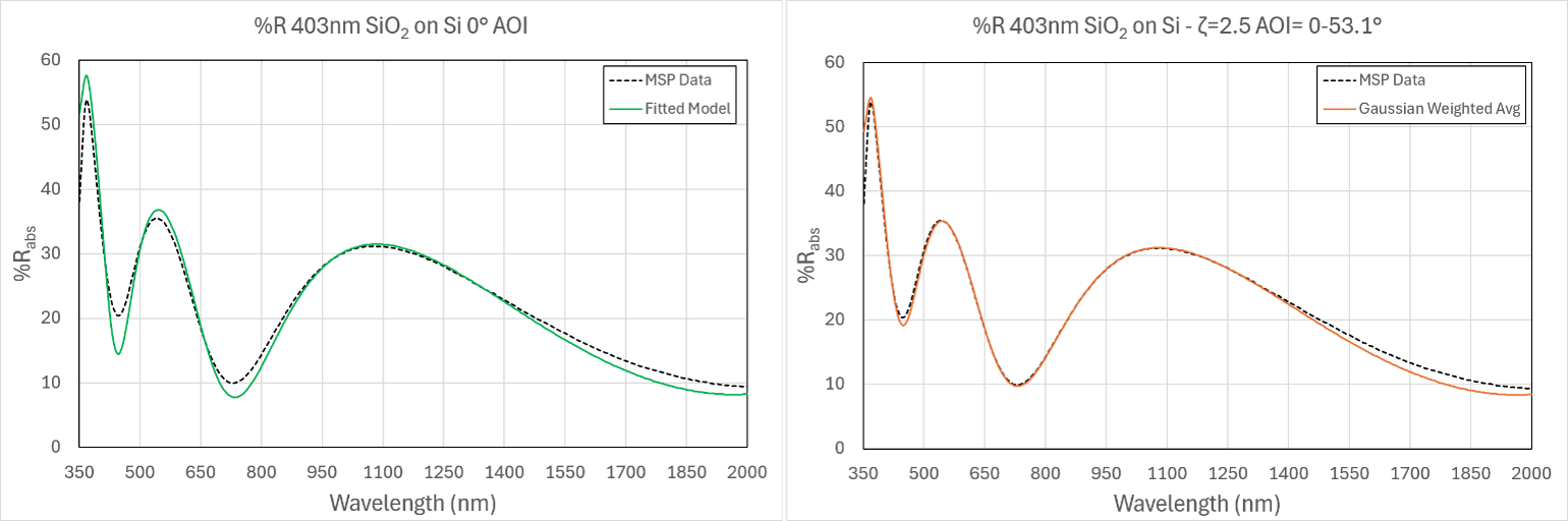
Figure 5. (Left) Measured spectrum (black-dash) of 403.6 nm SiO2 with modeled best fit (green) without incidence angle correction for thickness of 377.6 nm. (Right) Measured spectrum (black) of 403.6 nm SiO2 with modeled best fit (orange) including Gaussian-weighted incidence angle correction with zeta 2.5 for a thickness of 403.0 nm. Image Credit: CRAIC Technologies
As shown in Figure 5, omitting the incidence-angle correction significantly affects the modeled thickness values from the FilmPro software. Including these corrections improves the fit of the modeled spectra across the whole spectrum and yields more precise thin film thickness values.
However, these results apply only to flat samples and do not fully demonstrate CRAIC’s instruments' ability to measure curved surfaces. Reflectance spectra were also measured from a commercial collimation lens of a 785 nm laser.
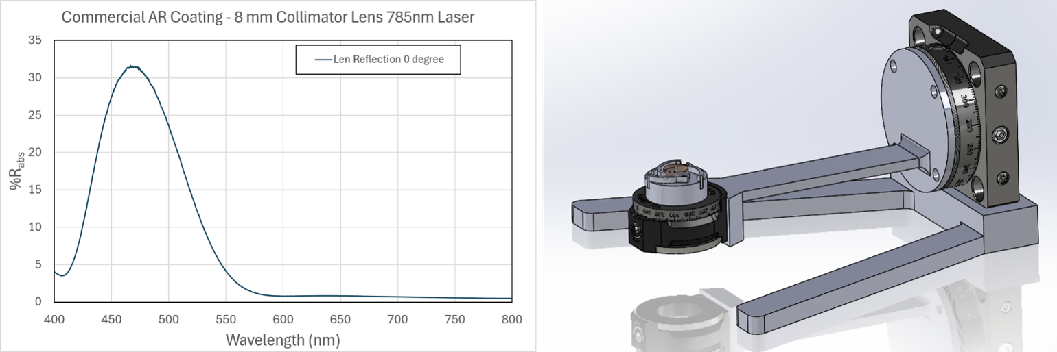
Figure 6. (Left) Spectrum of commercial AR coating on 8 mm lens for 785 nm laser collimation. (Right) Model of CRAIC’s small lens sample holder to allow for measuring ∼3.5 – 12 mm diameter lenses over nearly the whole curved surface of the lens, accomplished by the tilt and rotation adjustments, keeping the measurement area perpendicular to the incident light. Image Credit: CRAIC Technologies
Conclusions
By combining microscale spatial apertures to ensure local planar flatness, rejecting back-surface reflections via field-stop settings for peak confocal performance, and integrating incidence-angle distributions to match the objective numerical aperture, CRAIC’s microspectrophotometers deliver essential analytical capabilities for micro-optics production and quality assurance.
References
- Saigal, N., et al. (2014) Angle of incidence averaging in reflectance measurements with optical microscopes for studying layered two-dimensional materials. Review of Scientific Instruments, 85(7), 073105. DOI:10.1063/1.4889879. https://pubs.aip.org/aip/rsi/article-abstract/85/7/073105/355810/Angle-of-incidence-averaging-in-reflectance?redirectedFrom=fulltext.
- Schwarz, J., et al. (2023) Correlating optical microspectroscopy with 4 × 4 transfer matrix modeling for characterizing birefringent van der Waals materials. Small Methods, 7(10), 2300618. DOI:10.1002/smtd.202300618. https://onlinelibrary.wiley.com/doi/10.1002/smtd.202300618.
- Schwarz, J., et al. (2026) Complex refractive index determination via microspectroscopy through magnifying optics: Challenges and opportunities [Preprint]. arXiv. Avaialbe at: https://arxiv.org/abs/2607.03077.
Acknowledgments
Produced from materials originally authored by Dr. Jon Burdett, CRAIC Technologies.

This information has been sourced, reviewed, and adapted from materials provided by CRAIC Technologies.
For more information on this source, please visit CRAIC Technologies.