
Optical waveguides are structures designed to confine and guide light within a defined path. By controlling how electromagnetic waves propagate through a material, optical waveguides enable efficient, low-loss transmission of optical signals. They are widely used in fiberoptic communication for long-distance data transmission and are increasingly important in compact photonic devices where light must be routed, split, coupled, modulated, or detected within a small area.
In recent years, optical waveguides have become key building blocks in photonic integrated circuits (PICs). A PIC integrates multiple optical components - such as waveguides, couplers, splitters, modulators, filters, lasers, and photodetectors - onto a single chip to generate, guide, process, and detect light. PICs are used in applications such as optical communication, data center interconnects, sensing, LiDAR, quantum photonics, and other high-speed optical systems.
The performance of a PIC depends strongly on the physical dimensions of its waveguide structures. Parameters such as waveguide height, width, sidewall profile, trench depth, and coupler spacing directly affect optical transmission, coupling efficiency, propagation loss, and device-to-device uniformity. As PIC designs continue to shrink and include more closely spaced features, accurate dimensional metrology becomes increasingly important for process control, design verification, and device performance optimization.
The KLA Tencor® P-7, P-17, P-170, HRP®-260 and Zeta™-388 profilers provide the capability to measure these critical waveguide features, from long-range topographic scans to high-resolution measurements of individual waveguides and coupler structures.
Stylus Measurements
Photonic integrated circuits contain complex networks of waveguides that route and process optical signals. Because of the large physical size of these circuits relative to individual waveguide features, dimensional characterization is typically performed at multiple scales. A practical workflow begins with long-range scans to map the device topology, followed by localized 3D scans and 2D profiles to quantify critical dimensions, such as waveguide height, coupler gap, trench depth, and cross-sectional area.
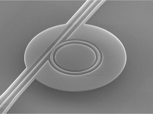
Figure 1. SEM image of a microring modulator structure in a photonic integrated circuit (PIC). Image Credit: S. K. Yeh et al., “Silicon Photonics Platform for Next Generation Data Communication Technologies,” 2024 IEEE International Electron Devices Meeting (IEDM). DOI: 10.1109/IEDM50854.2024.10873369.
A long-range 2D scan is first used to provide an overview of the PIC topology and identify regions of interest. This measurement helps verify waveguide continuity, understand the spatial relationship between photonic structures, and efficiently navigate to features that require higher-resolution characterization.
Figure 2 shows a 7 mm scan acquired using the KLA Instruments stylus profiler. Multiple waveguide features are resolved across the scan length as distinct peaks with heights greater than 400 nm. This overview scan functions as a roadmap of the device, enabling efficient selection of locations for detailed 3D imaging and cross-sectional analysis.
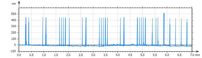
Figure 2. Long-range 2D scan of a lithium niobate PIC over a 7 mm scan length. Image Credit: KLA Instruments™
A 3D scan is generated from a series of closely spaced 2D profiles and provides a more complete view of the PIC surface topography. In Figure 3, the bottom left image shows a relatively large-area 3D scan of a 1100 µm × 600 µm region that includes several waveguides and a coupler structure. To examine the local geometry in greater detail, a high-resolution 3D scan was then performed on a smaller area. The top-right image in Figure 3 shows a fine scan of part of the coupler region, clearly resolving the change in gap between the two adjacent waveguides.
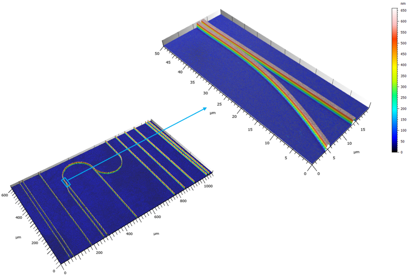
Figure 3. 3D scans of a lithium niobate PIC. The bottom-left measurement covers 1100 µm × 600 µm and captures the broader waveguide layout and coupling region, while the top-right scan covers 20 µm × 50 µm and provides a localized view of the waveguide spacing and topography. Image Credit: KLA Instruments™
To study coupler geometry in greater detail, a high-resolution 3D scan was performed at the center of the coupling region using a diamond DuraSharp® stylus. As shown in Figure 4, the measurement clearly resolves the two waveguide cores and the changing separation between them throughout the coupling region. The 3D topography provides direct visualization of waveguide shape, uniformity, and local process variations that may not be apparent from optical inspection alone.
In directional couplers, the spacing and parallelism of adjacent waveguides are critical because they directly influence optical coupling strength, power transfer efficiency, and splitting ratio. This measurement also enables evaluation of waveguide height uniformity and surrounding trench topography, providing valuable feedback for lithography and etch process optimization. The ability to obtain this information in a single non-destructive measurement makes stylus profilometry an effective metrology solution for coupler characterization during both process development and manufacturing.
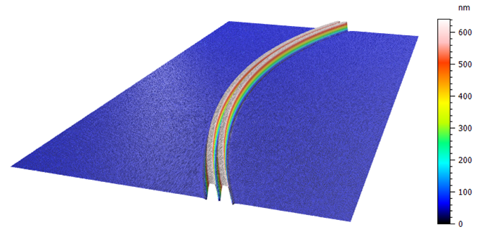
Figure 4. High-resolution 3D scan of the coupler structure illustrated in Figure 1, with a scan area of 50 µm × 90 µm. Image Credit: KLA Instruments™
While 3D scans provide comprehensive visualization of device topography, quantitative dimensional analysis is typically performed using extracted 2D profiles. Figure 5 shows measurements obtained from a profile crossing the coupler region, including waveguide height, coupler gap, trench depth, and cross-sectional area. These measurements provide direct access to the critical dimensions that determine optical device performance.
Waveguide height and width strongly influence optical mode confinement and effective refractive index. Even small dimensional variations can alter propagation characteristics and contribute to device-to-device variation. The gap between adjacent waveguides is particularly important in directional couplers because it governs the strength of evanescent-field interaction and therefore affects coupling efficiency and optical power distribution.
Area measurements further enable quantification of the overall waveguide cross-section, allowing engineers to monitor process uniformity and compare fabricated structures against design targets. By combining multiple measurement functions within a single profile analysis, stylus profilometry provides a rapid and comprehensive method for evaluating both process quality and device-critical dimensions. The high vertical resolution and constant-force control of the KLA Instruments stylus profiler enable accurate and repeatable characterization of these critical photonic structures.
Beyond individual device characterization, the automated Tencor P-170 and HRP-260 stylus profilers are also valuable for process monitoring and statistical process control. Measurements such as waveguide height and coupler spacing can be collected across multiple dies, wafers, or process lots to evaluate fabrication uniformity and detect process drift. The fully automated solution supports faster process development cycles, improved process understanding, and higher manufacturing yield for photonic integrated circuits.
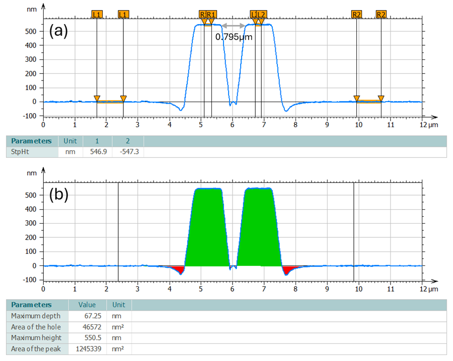
Figure 5. Quantitative profile measurements of the coupler structure. Image Credit: KLA Instruments™
Conclusion
The KLA Tencor P-7, P-17, P-170, HRP-260, and Zeta-388 surface profilers combine large-range scanning capability with high-resolution dimensional metrology in a single platform. From millimeter-scale device overview measurements to detailed characterization of waveguide and coupler structures, the systems provide the accuracy and flexibility required to support the development and manufacturing of next-generation photonic integrated circuits.
By enabling precise measurement of critical dimensions such as waveguide height, width, and coupler gap, the KLA profilers help ensure device performance and process consistency for advanced photonic applications.

This information has been sourced, reviewed, and adapted from materials provided by KLA Instruments™.
For more information on this source, please visit KLA Instruments™.