Why Pluggable Optics Struggle?
How Co-Packaged Optics Work?
Measuring the Power Savings
Current Engineering Challenges
From Prototypes to Production
Conclusion
References and Further Reading
Every time a question is sent to an AI chatbot, data races across thousands of processors via pulses of light in optical fibers. Inside data centers, switch chips manage this traffic, while specialized transceivers convert electronic bits into photons and back. As AI clusters expand, the energy consumption of these translations has climbed to a level that operators now treat as urgent.
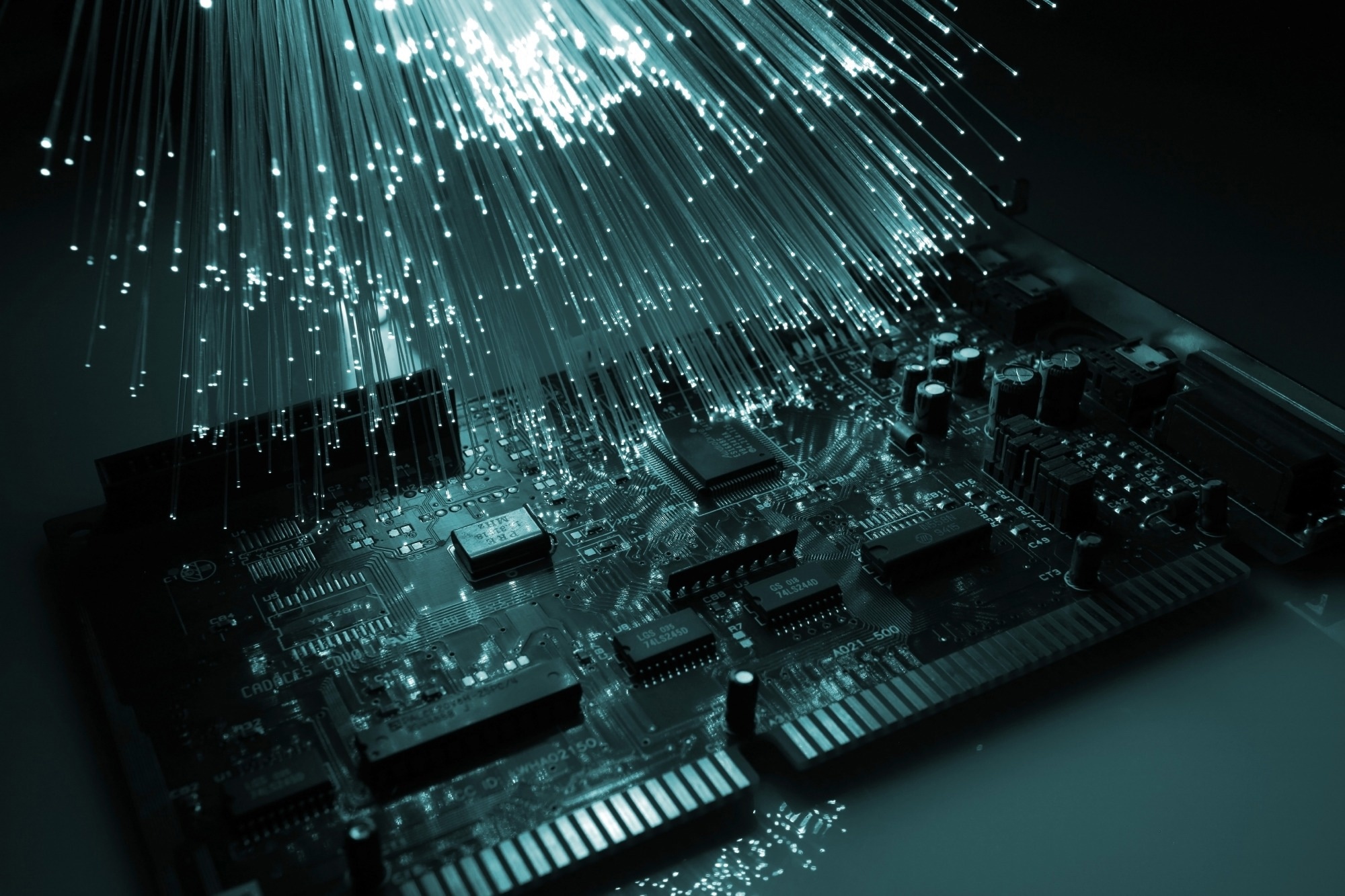 Image Credit: PeterPhoto123/Shutterstock
Co-packaged optics is an engineering response to that pressure. It aims to integrate light-handling components directly with processing chips. This article explores the limitations of conventional optical modules, the principles of co-packaged optics, and the current status of its commercial deployment.
Why Pluggable Optics Struggle?
In a network switch, the main chip is placed near the center of a circuit board, while pluggable optical transceivers fit into ports on the front panel. Each transceiver bundles lasers, optical circuits, and a digital signal processor into a compact module. Electrical signals travel several inches of copper traces on the board to reach these modules, and that distance becomes costly as data rates rise.1,2
Copper behaves like a leaky pipe at high signal frequencies. The circuits that send and receive data across these copper traces, known as SerDes, must apply heavy signal equalization to recover data bits distorted during the journey. In standard designs, signal loss along this path can exceed 20 dB, and compensating for it consumes extra power, adds latency, and limits how densely engineers can pack signals.3,4
Physical space further increases the complexity. A standard one-rack-unit panel holds only about 32 high-density pluggable ports, and switch chips have outgrown that capacity. Between 2010 and 2020, commercial switch capacity surged 40 times, increasing from 0.64 to 25.6 Tbps. The internal data center traffic also expanded at about 30% per year. Therefore, the front panel has become a congested bottleneck for modern switches.4
How Co-Packaged Optics Work?
Co-packaged optics reduces the length of electrical paths by placing small optical units right next to the switch chip in a shared package. In common designs, 4 or 8 silicon photonic chiplets surround a central processor, while optical fibers connect to the package itself. This setup can reduce the electrical distance between the chip and its optical converter to about 100 µm, about the width of a single human hair.3
Silicon photonics makes this integration easier because it uses the same manufacturing processes found in traditional computer chip production. Foundries can pattern waveguides, modulators, and photodetectors onto silicon wafers with high precision and repeatability. Engineers then join the photonic and electronic chips using advanced packaging methods such as through-silicon vias and silicon or glass interposers. These methods keep electrical connections short and dense.4,5
However, silicon has a key limitation. Its indirect bandgap makes it a poor light emitter, so lasers made from other semiconductor materials must supply the optical power. Most current designs place these lasers in a separate external module that feeds light into the package through a fiber. This setup allows technicians to replace a failed laser quickly and keeps the light source away from the switch chip's intense heat.1,2
Measuring the Power Savings
The case for co-packaged optics rests largely on energy per bit, which describes how much energy a system needs to move a single bit of data. Pluggable modules typically require 15 to 20 pJ/bit, while co-packaged systems operate at 5 to 10 pJ/bit. Researchers project that future designs could fall below 1 pJ/bit as integration and device design continue to improve.2,3
These figures carry real weight on a large scale. NVIDIA estimates that pluggable optics in a facility with 400,000 graphics processing units (GPUs) would consume about 40 MW, with lasers accounting for more than half of that load. Its co-packaged design uses one laser per 8 data links and cuts the total laser count by 25%. Operators can then redirect the saved power toward the GPUs that perform computation.1
Current Engineering Challenges
Heat management is the most critical issue in the integration of photonic and electronic devices. Switch chips can draw hundreds of watts, and the photonic devices beside them are highly sensitive to temperature. Most photonic components shift their operating wavelength by about 0.1 nm for every degree Celsius. Microring modulators, which Nvidia favors for their compact size, require built-in heaters and active control loops for optimal performance.1,3
Saving this for later? Download a PDF here.
Furthermore, connecting fibers to chips needs very high precision. A single-mode fiber core measures 8-10 µm in diameter, while a silicon waveguide is about 500X220 nm in size. This size difference requires alignment accurate to a fraction of a micron. A single switch may also require hundreds or thousands of fibers to be routed in tight bundles around its central chip, complicating assembly and increasing manufacturing costs.3,4
Integration also concentrates risk in one place. When optical engines share a package with an expensive switch chip, one faulty engine can compromise the entire assembly. Manufacturers, therefore, need very high yields for each component before final package assembly begins. Packaging engineers cite lasers as the leading source of defects in these complex systems, reinforcing the industry's preference for external, replaceable light sources in current designs.3,6
From Prototypes to Production
After years of laboratory demonstrations and pilot deployments, co-packaged optics has entered commercial production. Broadcom's 51.2-Tb Bailly switch has now reached volume manufacturing and reportedly cuts power consumption by up to 70% compared with conventional pluggable transceivers. NVIDIA has also begun shipping its Spectrum-X switches, built with TSMC packaging technology, to select partners, offering up to 400 Tbps of switching capacity.6
The pace of adoption will now depend heavily on supply chains. Optical engine manufacturing requires specialized expertise, and only a few suppliers worldwide can produce engines at high volume. Co-packaged switches also compete with AI processors for the same limited advanced packaging capacity. Analysts at TrendForce expect the market to reach its main volume ramp in 2027 and 2028, with vertically integrated vendors best positioned to capture demand.6
Conclusion
Co-packaged optics addresses a physical problem that grows with every generation of data center hardware. By moving optical conversion next to the switch chip, it shortens lossy copper paths, frees up panel space, and reduces the energy required to move each bit. Thermal control, fiber alignment, and manufacturing yield still demand careful engineering. As commercial shipments scale, co-packaged optics is poised to become the standard for how AI data centers move information efficiently.2,6
References and Further Reading
- Samuel K. Moore. (2025). A Crucial Optical Technology Has Finally Arrived: Nvidia’s endorsement of co-packaged optics means the time is right. IEEE Spectrum. https://spectrum.ieee.org/co-packaged-optics
- Tian, W. et al. (2024). Progress in Research on Co-Packaged Optics. Micromachines, 15(10), 1211. DOI:10.3390/mi15101211. https://www.mdpi.com/2072-666X/15/10/1211
- Laura Peters. (2025). Co-Packaged Optics Reaches Power Efficiency Tipping Point. Semiconductor Engineering. https://semiengineering.com/co-packaged-optics-reaches-power-efficiency-tipping-point/
- Tan, M. et al. (2023). Co-packaged optics (CPO): Status, challenges, and solutions. Frontiers of Optoelectronics, 16(1), 1. DOI:10.1007/s12200-022-00055-y. https://link.springer.com/article/10.1007/s12200-022-00055-y
- Chen, G. et al. (2025). Electronic Chip Package and Co-Packaged Optics (CPO) Technology for Modern AI Era: A Review. Micromachines, 16(4), 431. DOI:10.3390/mi16040431. https://www.mdpi.com/2072-666X/16/4/431
- NVIDIA and Broadcom Begin Volume Ramp of CPO Switches, with Optical Engine Yield and Advanced Packaging Capacity Emerging as Key Expansion Bottlenecks, Says TrendForce. (2026). TrendForce. https://www.trendforce.com/presscenter/news/20260727-13151.html
Disclaimer: The views expressed here are those of the author expressed in their private capacity and do not necessarily represent the views of AZoM.com Limited T/A AZoNetwork the owner and operator of this website. This disclaimer forms part of the Terms and conditions of use of this website.