Mar 2 2010
A new device invented by engineers at UC Davis could make it much faster to convert pulses of light into electronic signals and back again. The technology could be applied to ultrafast, high-capacity communications, imaging of the Earth's surface and for encrypting secure messages.
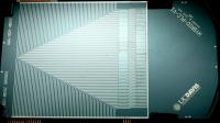 The faint tree-like structures visible on the right side are optical waveguides that bring the light into and out of the optical circuit
"We have found a way to measure a very high capacity waveform with a combination of standard electronics and optics," said S.J. Ben Yoo, professor of electrical and computer engineering at UC Davis. A paper describing the technology was published Feb. 28 in the journal Nature Photonics.
The device is up to 10,000 times faster than existing technologies for measuring light pulses, Yoo said. It overcomes the limitations of existing approaches, by measuring both the amplitude (intensity) and the phase of a pulse at the same time, and can measure information capacity into the 100 terahertz range in real time. Current electronics are limited to information capacity in tens of gigahertz bandwidth.
Higher-frequency pulses can pack more information into a given length of time. By making it possible to take a complex waveform and quickly decode it into a digital electronic signal, the device would make it possible to pack more data into optical signals.
Operated in reverse, the same kind of device could be used to generate optical signals from electronics.
The device -- developed by Yoo's UC Davis research group, including graduate student Nicolas Fontaine; postdoctoral researchers Ryan Scott, Linjie Zhou and Francisco Soares; and Professor Jonathan Heritage -- divides the incoming signal into slices of frequency spectrum, processes the slices in parallel and then integrates them.
The technology could be used in ultra-high-speed communications and also in LiDAR (light detection and ranging) systems. LiDAR uses pulses of laser light to rapidly scan the landscape and produce highly detailed, three-dimensional images of the Earth's surface.
The next step is to work on putting the whole device into a small silicon chip, Yoo said.