Gallium nitride (GaN) based devices are attractive for harsh environment electronics because of their high chemical and the mechanical stability of GaN itself that has a higher atomic displacement energy than other semiconductor materials.
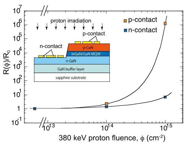 This image depicts two-terminal resistance of p- and n-type GaN as a function of proton fluence. This inset shows schematic of sample, and lines are guide for eyes. Credit: copyright (c) 2014 Toyohashi University of Technology. All rights reserved.
However, degradation mechanisms of GaN device under radiation environments is not clear mainly because devices consist of many different types of semiconductors, such as p-type and n-type layers in light emitting diode (LED), and each layer has different hardness to radiation.
Now, researchers at the Electronics-Inspired Interdisciplinary Research Institute (EIIRIS) and Department of Electrical and Electronic Information Engineering at Toyohashi University of Technology, and the Japan Atomic Energy Agency (JAEA) describe the physical mechanism of an observed increase in the resistance of p-type GaN irradiated with 380 keV protons compared with n-type GaN.
The GaN-based LED structure shown in Fig.1 was irradiated with protons and the resulting electrical properties measured. Notably, the electrodes to measure the resistance of the p-type and n-type layers were produced independently using the clean room facilities at EIIRIS and the ion implanter in JAEA.
The two terminal resistance of the n-type GaN did not vary from its initial value after 1x1014 cm-2 proton irradiation, and remained of the same order after 1x1015 cm-2 protons. However, a clear increase of the resistance was found in the p-type GaN after 1x1014 cm-2 irradiation. The resistance increased further by six orders of magnitude after 1x1015 cm-2.
The observed increase of the resistance in p-type GaN is explained as being due to the lower initial carrier density than in n-type GaN due to a lack of efficient p-type doping technology for GaN, which is a key for the realization of novel devices operable in harsh environments.