Sponsored by HORIBAReviewed by Olivia FrostMar 26 2026
Research conducted over the last decade has transformed tip-enhanced Raman scattering (TERS) from a technique once widely regarded as ‘niche’ to a popular and routine nanoscale characterization method.1
TERS continues to see widespread and beneficial use in the analysis of nanoscale heterogeneities and defects in two-dimensional semiconductors, for example, transition metal dichalcogenides and their Janus compounds.
These materials have attracted considerable attention from the research community due to their intriguing optoelectronic properties. Excitons mediate these properties at strong binding energies (hundreds of meV), able to survive at RTP.
The Raman spectra of TMDs have been shown to change dramatically as a function of the excitation laser wavelength, with Raman modes of different origins (first- vs second-order Raman bands) potentially following different excitation profiles.2
TERS has enabled the correlation between the appearance of a specific spectrum and a specific nanoscale feature, such as a mono- or multilayer or a lateral and vertical heterostructure.
Most TERS imaging experiments are performed when the tip is in direct mechanical contact with the sample (permanent or intermittent); however, this means that the probe’s structure and enhancement factor may shift during the imaging procedure.
This makes it potentially difficult to confirm whether detected differences in TERS spectra are related to the material’s intrinsic properties or whether these can be attributed to the changes in TERS probe properties, which impact the quality and reproducibility of the imaging.
HORIBA has developed a methodology to address this concern. The company’s approach sees TERS imaging performed with two lasers at the same time, with the Raman response also collected for both excitation wavelengths.
This method ensures that any differences in TERS response across excitation wavelengths relate solely to the material's optical properties, rather than to the TERS probe or sample degradation.
This approach reduces acquisition time (by collecting two maps at once) while also extending the lifetime of the TERS probe.
Concurrent Laser Illumination Setup on the LabRAM Odyssey Nano
The LabRAM Odyssey from HORIBA is an exceptionally customizable and flexible instrument able to accommodate virtually any research requirements.
The example presented here used an experimental setup designed to perform TERS, alongside a special set of accessories to enable concurrent bi-laser excitation.
The setup featured standard coupling to an atomic force microscope (AFM) via an optical platform (OmegaScope) (Figure 1), including an external 785 nm laser redirected inside the OmegaScope with a 10 % reflective beam splitter, and the internal 633 nm laser. A beam dump collects the transmitted part of the 785 nm beam.
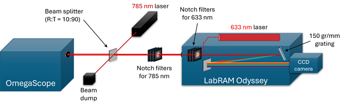
Figure 1. Schematic view of the LabRAM Odyssey Nano (coupled with the AFM via an OmegaScope) with the concurrent bi-laser excitation setup. Image Credit: HORIBA
Once the two lasers have reached the AFM probe, the back-scattered signal passes through two sets of Notch filters, one external filter for damping the intensity of the 785 nm line, and one internal filter to the LabRAM for the 633 nm line.
The signal is diffracted by a 150 gr/mm grating once it is inside the spectrometer. This maximizes the spectral collection range and records contributions from the two laser lines.
This method ensures comparability of the recorded spectra. These spectra are collected in the same experimental conditions, minimizing overall measurement time and preventing any laser-induced probe and/or sample modification during analysis.
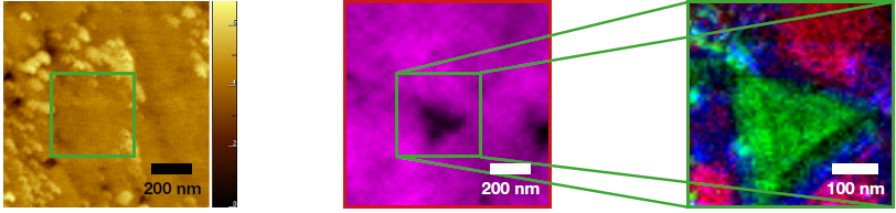
Image Credit: HORIBA
A silver-coated probe was used to perform AFM-TERS analyses on a sample comprised of WS2 flakes. This sample was deposited on a silver substrate.
The flakes’ thickness is sub-nanometric, resulting in the formation of a plasmonic cavity between the silver probe and substrate. This ‘gap mode configuration’ helps to improve the TERS effect.
Figures 2a and 2b feature the results of a Kelvin-FM measurement performed prior to TERS analysis. Flakes are virtually invisible in the Height map (Figure 2a) in this instance, but they can be recognized in the CPD map (Figure 2b) by their different work function relative to the metallic substrate.
Next, a TERS mapping (Figure 2c) was performed in the area around the triangular-shaped flake (Figures 2a and 2b, dotted line). The color code shown in the map is created by integrating different bands in each zone’s average spectra (Figure 2d).
Spectra in the green zone exhibit a sharp A1g band, which corresponds to the WS2 bilayers. The red zones feature the A’/A1 doublet, which indicates the presence of a WS2 monolayer.
These three signals coexist in the blue areas, potentially suggesting a mixed mono/bilayer structure concentrated at the edge of the bilayer flake.
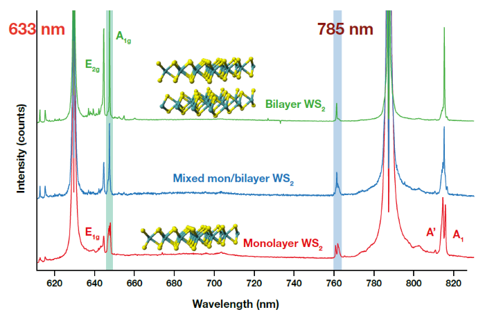
Figure 2. (a) Height and (b) CPD (contact potential difference) maps acquired on WS2 in Kelvin-FM mode. (c) TERS hyperspectral map, acquired inside the area surrounded by the dotted lines in (a) and (b) with the concurrent excitation of the 633 and 785 nm lasers (0.2 s/pixel). (e) Average spectra for the different coloured zones of the TERS map, obtained by integration of the A1g (green), A’ (red), and A1 (blue) bands, respectively. Please note that the X-axis is given in nm because the Raman shift (in cm-1) is not the same for the two lasers. Image Credit: HORIBA
It is important to note that the spectra obtained from the two lines on the same structures are not exactly identical. For example, the bilayer’s E2g band is very strong with the 633 nm laser, but this band does not exist in the 785 nm spectrum, in a similar manner to the monolayer’s E1g band.
The intensity of the A’ band is more prominent with the 785 nm laser, where it can be clearly seen from the anti-Stokes bands, despite being very weak with the 633 nm laser.
This difference highlights the importance of completing resolved and comparable spectral analysis on WS2 via multiple laser lines.
A recent study done with an identical illumination setup revealed the precise influence of the excitation energy on the A’/A1g of different WS2 and MoS2 structures.3
The ability to study these types of behaviors with a rapid, accurate, and extremely resolved instrumental setup could potentially lead to new and exciting discoveries throughout the nano-optoelectronics field.
References and Further Reading
- S. A. Saunin, A. V. Krayev, V. V. Zhizhimontov, V. V. Gavrilyuk, L. N. Grigorov, A. V. Belyaev, D. A. Evplov Systems and Methods for Non-Destructive Surface Chemical Analysis of Samples, US Patent US20150338439A1
- del Corro, E., et al. (2014). Excited Excitonic States in 1L, 2L, 3L, and Bulk WSe2 Observed by Resonant Raman Spectroscopy. ACS Nano, 8(9), pp.9629–9635. DOI: 10.1021/nn504088g. https://pubs.acs.org/doi/10.1021/nn504088g.
- Krayev, A., et al. (2025). Excitation Laser Energy Dependence of the Gap-Mode TERS Spectra of WS2 and MoS2 on Silver. ACS Photonics, (online) 12(3), pp.1535–1544. DOI: 10.1021/acsphotonics.4c02257. https://pubs.acs.org/doi/10.1021/acsphotonics.4c02257.
Acknowledgments
Produced from materials originally authored by HORIBA.

This information has been sourced, reviewed, and adapted from materials provided by HORIBA.
For more information on this source, please visit HORIBA.