A new type of advanced microscope (wide-field coherent multidimensional microscopy) has been developed. It uses a carefully designed sequence of ultrashort light pulses to study the behavior of high-tech materials, with potential practical applications in the study of innovative materials such as those used to build solar panels. This is the result of work by a research group of physicists from the Faculty of Sciences, Mathematics, Physics, and Natural Sciences at Università Cattolica’s Brescia campus who, for the first time, have developed a “multidimensional microscope” that, in a sense, records the behavior of materials.
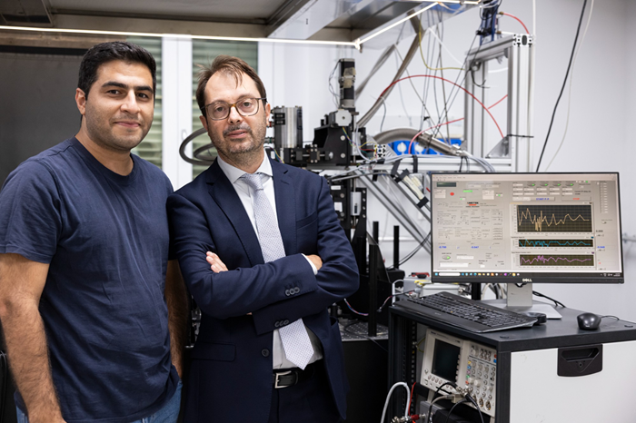 Image Credit: Università Cattolica del Sacro Cuore
The study was published in the journal Optica and coordinated by the dean of the faculty, Professor Claudio Giannetti, director of the Interdisciplinary Laboratories for Advanced Materials Physics (ILAMP).
The new microscope can track phenomena that occur over incredibly short time frames, on the order of a few millionths of a billionth of a second. To achieve this, the microscope uses extremely short laser light pulses and observes the material’s reaction step by step in order to understand the mechanisms of electron interaction in different regions of a microelectronic device.
The Study
This type of microscope was developed for the first time at the ILAMP laboratories in Brescia, in collaboration with Politecnico di Milano, KU Leuven, the University of British Columbia, and the CNR. It works by creating a sequence of identical light pulses that illuminate a sample placed inside the microscope. This is the most delicate part of the process and was developed in collaboration with NIREOS S.r.l., a spin-off of Politecnico di Milano that specializes in new photonics solutions.
Scientists tested the new microscope on a device consisting of a small sheet of tungsten diselenide just a few atomic layers thick. This graphene-like material is of great interest in optoelectronics because of its unique optical and electronic properties. The researchers observed how the material’s properties vary depending on its position within the microdevice, providing insight into the mechanisms that prevent electrons from moving freely.
Possible Practical Applications
The microscope could be used, for example, to identify imperfections that might compromise a device’s efficiency in electrical transport and energy exchange. Information of this kind could help in designing more efficient solar cells, as well as faster LEDs, sensors, and electronic devices.
The technique could also be useful in studying biological systems and the metabolism of cancer cells, in synergy with other research projects at the center (Q-META).
Conclusions
This result marks the beginning of a new field of research in which ILAMP is working to understand how to observe and control the quantum properties of a material, thereby paving the way for the development of new systems to form qubits, the building blocks of quantum computers, that operate at temperatures several orders of magnitude higher than current technology and at speeds 1000 times faster.