Mar 4 2019
Researchers of the University of Twente (UT) have discovered a tiny prison for photons, or nanocavity. An optical crystal—a structure of pores etched in two perpendicular directions— surrounds the very small cavity. Restraining photons in this 3D cavity may pave the way to miniature and efficient lasers and LEDs, ultrasensitive light sensors, or storage of information. The findings are reported in Physical Review B, one of the journals of the American Physical Society.
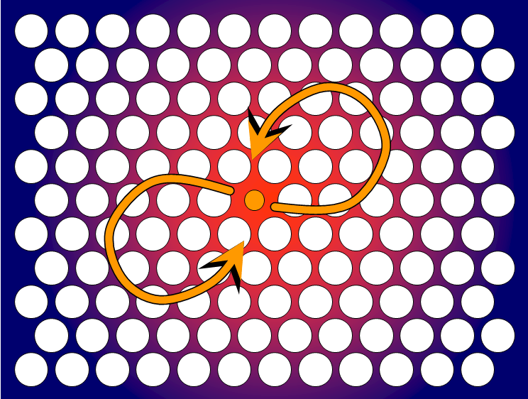 A deliberately created 'defect' in a photonic crystal forms a cavity from which a photon cannot escape. (Image credit: University of Twente)
Methods for capturing light are at the fundamentals of photonics. A well-recognized cavity consists of two mirrors between which a standing wave will be developed of a particular color of light, subject to the distance between the mirrors. This is the working norm of a laser. But light that is seeping sideways cannot be reflected again. Will it be possible to capture a photon inside a 3D “prison cell” surrounded by mirrors? It certainly is, the UT scientists now prove. The mirrors, in this case, are created by a 3D photonic crystal, comprising of pores that have been etched deeply into silicon in two directions, vertical to each other.
Photonic crystals are recognized for their extraordinary light properties. The structure and periodicity of the pores permit only light of specific wavelengths to spread inside the crystal. But how can one create, in a structure similar to this, a cavity for capturing a photon?
In their latest paper, the UT scientists show that this is feasible by purposely altering the diameter of two pores. At their crossing point, an abnormality or defect forms within the crystal. This minute cavity is surrounded by the intermittent crystal structure, pushing the photon back into the cavity. There just is no escape.
Our calculations show that in this tiny volume of the cavity, the optical energy is enhanced by up to 2400 times compared to the outside of the crystal. This is a very large enhancement, given the small dimensions.
Dr. Devashish, Study Lead Author, UT.
Lightweight
By changing the periodic structure in the vicinity, the crystal also displays substantial absorption of visible light, up to ten times the absorption of bulk silicon. “This strong absorption, in a very tiny volume, is a great property for new sensors. Thanks to the high density of pores, the crystal is very lightweight—we also call this ‘holeyness’”, Prof Willem Vos says. He is the Complex Photonics Systems group leader at UT’s MESA+ Institute.
In previous publications, the team demonstrated that diamond-like photonic crystals can reflect a very wide range of colors of light for all angles: these results brought forth the new discovery currently presented. In the forthcoming generations of photonic integrated circuits (PICs), the nanocavities are projected to play a huge role in quantum photonic devices, the treatment of optical signals, or in information storage.
The study was done by the Complex Photonic Systems group, along with the Mathematics of Computational Science group, both UT’s MESA+ Institute.