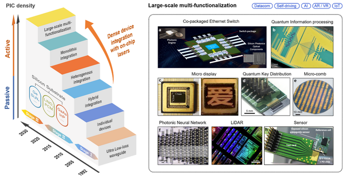
Examples of Large-scale multi-functionalization are listed: a Co-packaged Ethernet Switch. b Quantum Information processing. c Micro display. d Quantum Key Distribution (QKD). e Micro-comb. f Photonic Neural Network. g LiDAR. h Sensor. Image credits: Zhican Zhou, Xiangpeng Ou, Yuetong Fang, Emad Alkhazraji, Renjing Xu, Yating Wan, and John E. Bowers
A research group headed by Prof. Yating Wan from KAUST and Prof. John Bowers from UCSB has published a new study in eLight that sheds light on the prospects of on-chip lasers. They examined the probable applications in their study.
In transitioning from assembled optics to on-chip photonics with compact form factors, silicon becomes an obvious choice due to its superior optical properties and compatibility with the mature complementary metal-oxide-semiconductor (CMOS) technology.
The large difference between silicon and silicon dioxide enables photonic devices to be made in a compact size. The series of optical components established on the silicon-on-insulator (SOI) platform is very attractive. Silicon, however, has a low emission efficiency. On-chip light sources fell far behind silicon-based photonic devices and turn out to be a hindrance to mass production.
In the field of on-chip light sources, many studies have emerged in the past few decades. In this study, the authors concentrate on the on-chip incorporation of the main element in PIC: an energy-efficient, compact, and strong laser source. They begin with an outline of the decades of efforts in discovering new materials and integration technologies for on-chip lasers, which include heterogeneous, hybrid, and monolithic integration.
Creating above $1 billion of revenue, more than six million 100-gigabit optical modules with heterogeneously integrated on-chip lasers have been sent by Intel. Considerable enhancements in III-V/Si epitaxy have furthered quantum dot (QD) technology to the frontlines of silicon photonics in monolithic integration.
In spite of the material incompatibility between silicon and III-V, the large tolerance to material defects enables successful device operation. In PICs, the much-reduced reflection sensitivity feedback provides the probability of avoiding optical isolators. These record-low threshold currents and the high-temperature stability of lasers offer several novel probabilities.
Also, many paths have been discovered for active-passive coupling and co-integration of QD lasers to the remaining parts of silicon photonics. A monolithic offset QD integration platform has been developed, which allows the creation of a laser cavity using both the flexibility of passive GaAs waveguide structures and resilient QD active region.
Promising results are shown by a heterogeneous QD integration platform. A synergistic relationship between the III-V QDs and silicon results in superior devices surpassing what is possible with purely III-V QD devices. Enabling commercial relevance, this method will scale photonic integrated circuits to 300 mm or even 450 mm diameter wafer size for high-volume applications.
Datacom is still the largest driver in the advanced development of silicon photonics. Dense device integration with on-chip lasers, however, will be important for numerous planned future applications.
The authors examine the corresponding material system compatibility and efficient energy channeling from device to device on-chip in the second part of the study. The study concentrates on the advantages and possible application of on-chip lasers in several functionalized PICs, along with optical communications and interconnects, chemical and biological analysis, optical phased array-based LiDAR, and sensors.
The outlook of silicon integrated circuits and silicon photonics was unquestionably too fascinating. It is mainly due to their capacity to utilize and effortlessly combine with the already matured high-quality CMOS fabrication technology. CMOS fabrication technology can gain high-volume productions at low die-costs, along with outstanding uniformity and a great degree of scalability.
Multiple solutions to overcome limitations through the years were driven by a lot of research and development from the industry and academia.
As time has passed, novel methods have been conceived. In fact, today, several chip-level devices have matured based on silicon photonic processes for different applications integrating on-chip lasers by various integration techniques.
However, the design and process routes of major manufacturers still differ considerably. From this perspective, PIC technology is still in its early stages, where the final solution with the ideal cost-performance-reliability balance is yet to set a record.
Journal Reference
Zhou, Z., et al. (2023) Prospects and applications of on-chip lasers. eLight. doi.org/10.1186/s43593-022-00027-x.