Researchers at the North Dakota State University’s (NDSU) Center for Nanoscale Science and Engineering have developed a new wafer-to-product electronics manufacturing technology that can reduce the unit cost and size of microelectronic devices.
 Researchers at North Dakota State University, Fargo, say a new electronics manufacturing technology developed at its Center for Nanoscale Science and Engineering eliminates challenges facing conventional packaging techniques and shows promise to significantly reduce the size and unit cost of microelectronic devices.
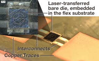
The innovative laser-enabled advanced packaging (LEAP) technology omits the difficulties faced by customary packaging techniques. It is an all-inclusive technology that enables non-contact assembly of ultrathin semiconductor chips onto flexible and rigid substrates with lower cost, and higher throughput.
The research group for advanced electronics packaging at the NDSU has been developing the LEAP technology from 2008. They had earlier fabricated an electronic device having an ultra-thin silicon chip, laser-assembled and embedded in a flexible type of substrate.
The Thermo-Mechanical Selective Laser Assisted Die Transfer (tmSLADT) process is a critical part of the LEAP technology. With high accuracy it has the ability to place ultra-thin semiconductor chips smaller than 50 µm at specific orientations and selective locationson the flexible substrate. NDSU CNSE’s associate director for electronics technology, Aaron Reinholz, stated that the tmSLADT process and the LEAP technology enable interconnection and high-volume placement of different types of fine pitch, ultra-thin, passive and active circuit components, which allow devices comprising of flex substrate electronics to be manipulated, rolled, and bent.
The tmSLADT process can also be used in other micro-assembly and microelectromechanical system (MEMS) fabrication applications. In addition to defense applications, the LEAP technology can be used in single-chip devices including “smart” bank notes, smart cards, RFID tags, bank cards, self-adapting conformal antennas, intelligent sensors platforms and such disposable and flexible microelectronic devices.