Global data demand continues to grow at an exponential rate, driven by emerging applications in cloud computing, artificial intelligence, autonomous systems, and high-bandwidth communications. Even during the 2020 COVID-19 pandemic, global network traffic rose by more than 20 %, underscoring the critical importance of scalable, energy-efficient data transmission and routing infrastructure.
The photonics chip industry continues to expand rapidly, with its technologies now integrated into a broad spectrum of mainstream applications. These include advanced light detection and ranging (LiDAR) systems, compact sensor modules in wearables and automotive vision systems, and emerging fields such as quantum information processing, high-speed optical interconnects, and photonic computing, where photons replace electrons as information carriers for logic operations.
At the core of this technological transformation lies silicon photonics (SiPh) - a platform that monolithically integrates optical and electronic functionality on a single silicon substrate. This integration provides substantial benefits in bandwidth density, energy efficiency, and form factor reduction.
Given the rapid diversification of SiPh applications and the accelerating adoption in consumer and data-communications markets, production volumes are projected to increase by several orders of magnitude - potentially up to a thousand-fold - in the coming years. Achieving this scalability will require equally transformative advances in automated optical alignment and packaging technologies, which are the focus of this discussion.
The Difference Between Optical and Electronic Alignment
Compared to electronic ones, optical circuits require more time-consuming verification and characterization steps at multiple stages - from wafer-level testing through subsequent packaging and assembly processes. Each stage demands positional accuracies that are typically two to three orders of magnitude tighter than those required for conventional electronic probing and often involve additional mechanical degrees of freedom (DOF).
In electronic testing, probe needles can readily contact electrical test pads, with feature sizes on the order of tens of micrometers. In contrast, silicon photonics (SiPh) test structures and coupling interfaces present optical features with alignment tolerances in the 20–50 nm range. Achieving and maintaining this level of precision necessitates advanced motion systems at the nanometer level and closed-loop control architectures far beyond those used in traditional semiconductor probing.
Such precision cannot be realized through passive visual feedback - microscope- or camera-based alignment methods, which lack the necessary spatial resolution and dynamic feedback speed. Consequently, optical alignment must be active, relying on real-time optimization of coupled optical power to determine true alignment. This approach ensures maximum transmission efficiency despite mechanical, thermal, or process-induced variations.
The Challenge of Upscaling SiPh Production
Fabricating photonic integrated circuits requires challenging nanopositioning tasks, and vision- or fixturing-based techniques are insufficient, especially given device variances.
The requirement for repetitive alignment throughout all manufacturing stages, from initial probing and grading on the wafer to final assembly and packaging, which includes multiple steps of placing and bonding functional elements interspersed with additional testing, has long been regarded as a barrier to scaling up production, accounting for up to 80% of total costs.
The historically high expense of active alignment methods has been a primary motivator for the multi-decade hunt for passive alignment technology. Precision active alignment is now available, eliminating numerous associated expenses and allowing for a cascade of savings throughout the manufacturing workflow.
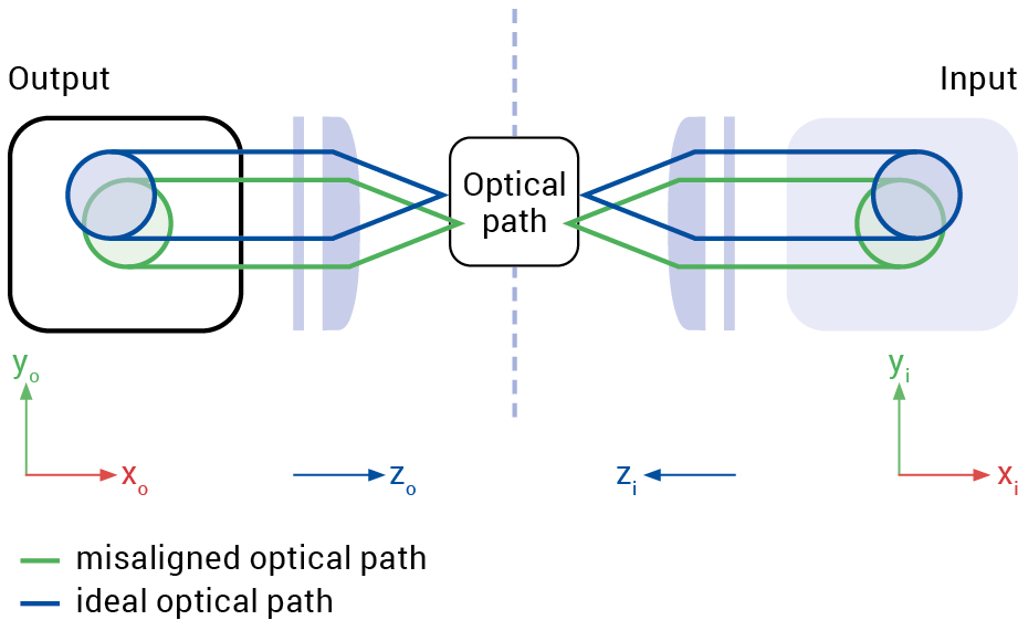
Figure 1. Testing and packaging today’s photonic devices can be challenging across multiple DOF. The alignment of multi-channel devices, such as fiber-optical arrays, used to be a slow, repetitive process before modern parallel algorithms were developed. Image Credit: PI (Physik Instrumente) LP
Passive or Active Alignment?
An active or passive technique can accomplish precision alignment in non-photonics manufacturing. A dovetail joins two boards at right angles, aligning the edges.
Passive positioning, however, is often ineffective for applications needing higher accuracy, such as aligning optical fibers to chips or other components, because the tolerances are too tight, making manufacturing processes unstable.
When the design becomes more sophisticated, the machine tools and procedures needed to meet the requisite tolerances become more expensive, and the number of rejects increases, resulting in additional expenditures.
Some device tolerances, such as fiber-core centration, cannot be addressed with improved fabrication techniques, and machining the world's finest V-groove is of little use when device-to-device variability exceeds the required alignment tolerances.
Ingenious passive alignment solutions have arisen that show great promise for specialized applications, such as the Photonic-Plug (Teramount), although active alignment will remain necessary.
In comparison, active alignment enhances performance by using robots to autonomously align devices, and given the cost savings, flexibility, and speed indicated below, it will continue to be the favored choice for photonic device manufacturing in the future.
Active alignment works by maximizing coupling performance, and the latest breakthrough detailed in this research does so cost-effectively across multiple channels in different DOF, which is necessary because SiPh can print several circuits with multiple inputs and outputs on a single chip.
Active Alignment: What is Necessary?
Active alignment necessitates advanced control electronics and high-precision mechanics. During manufacturing, the photonic device's components are autonomously controlled to maintain their mutual position.
Traditionally, this was a time-consuming operation since optimizing several channels, inputs, and outputs in multiple DOF needed numerous iterations to achieve the desired result. Using old methodologies, this time will only increase as devices become smaller and more complex, raising the cost even higher.
For example, alignment in a multi-lens assembly is significantly more difficult than for a single element, as is a SiPh chip with several channels instead of the single fibers used in the late 1990s.
Fortunately, revolutionary control algorithms can now simultaneously complete all of the necessary sub-alignments across various DOF, channels, and operating systems, completing the entire operation in a single rapid step. This eliminates repetitive looping and often lowers alignment time by 99%.
Precision Positioning of Signal-Carrying Elements
The primary problem in active alignment is precisely arranging signal-carrying devices, such as single fiber or fiber arrays, lenses, interposers, or other chips, in relation to coupling points like grating couplers or edge facets.
These couplings can occur within or outside passive and active photonic structures such as waveguides, vertical cavity surface-emitting lasers, and photodiodes. When linking photonic components, alignment accuracy of tens of nanometers is typically required to achieve the maximum optical power transmission and lowest attenuation.
Precision Automation: Finding the Main Peak
In almost all photonic component alignments, the signal, such as linked optical power, reaches a global peak when optimally aligned and declines when out of place.
This is a global pattern, and spurious lower or local peaks are frequently observed, which should not be chosen for optimization. However, finding that global peak has typically been time-consuming, especially when it involves many DOF.
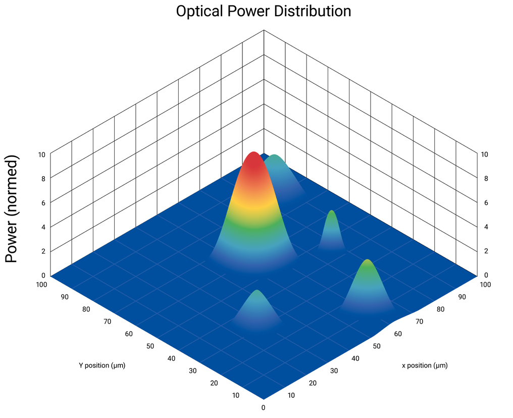
Figure 2. Power distribution of an optical component shows multiple peaks. Modern algorithms and precision mechanics can help determine the main mode and find the exact peak quickly. Image Credit: PI (Physik Instrumente) LP
Advanced Algorithms and Fast Mechanics
A revolutionary combination of advanced algorithms and quick mechanisms, such as PI's award-winning Fast Multichannel Photonics Alignment solutions (FMPA), has significantly increased throughput.
FMPA optimises coupling between photonic elements across channels, inputs and outputs, and DOF, even when these independent variables influence each other, using novel functionalities such as rapid first light detection, a vibrationless areal scan, and an innovative parallel gradient search capable of real-time, multivariate tracking optimization.
Previous approaches required coupling to be tuned sequentially, looping back and forth, and readjusting at each axis to gradually establish a consensus.
This took a long time, sometimes several minutes, and had a substantial influence on costs, efficiency, and scalability. In comparison, FMPA can make all of these changes in a single step using a simple set of commands that take only seconds to execute.
Because the alignments are executed concurrently, the optimization time is substantially independent of the number of alignments. This considerable reduction in alignment time, generally two orders of magnitude, dramatically lowers costs, making operations like probing SiPh wafers commercially viable.
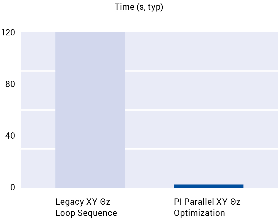
Figure 3. Alignment speed is crucial in reducing production costs. Image Credit: PI (Physik Instrumente) LP
Active Alignment: Different Processes
There are two types of alignment methods for photonic components: area scans and gradient searches.
Areal scans identify the peak of a measured figure of merit, such as optical power, modulation transfer function (MTF), or modal purity, within a specific region. They can be used to precisely characterize a component's optical fingerprint and differentiate global and local maxima.
Gradient searches allow for quick final optimization and tracking, and FMPA's unique implementation may optimize and track one or more couplings in several DOF at the same time, reducing drift processes, disturbances, and so on. These steps are covered in greater depth below.
Area Scans
Areal scans, which scan an area to discover the approximate location of the highest coupling peak, are used for a variety of purposes, including:
- Detecting the earliest light
- Profiling a coupling for effective process control
- Localizing a coupling's principal mode for optimization using gradient search. This sequence creates a powerful hybrid strategy that helps prevent locking upon a local maximum.
FMPA's area scans include unique single-frequency sinusoid and spiral scans. These are substantially faster than raster or serpentine scans because they are continuous and do not require the stop-and-start actions that traditional scans do.
In addition, the frequency is adjustable to avoid generating structural resonances. It is also possible to pick a constant velocity spiral scan, which allows data to be acquired with a constant density throughout the spiral.
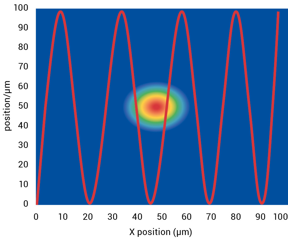
Figure 4a. Sinusoidal areal scan for detecting first light. Image Credit: PI (Physik Instrumente) LP
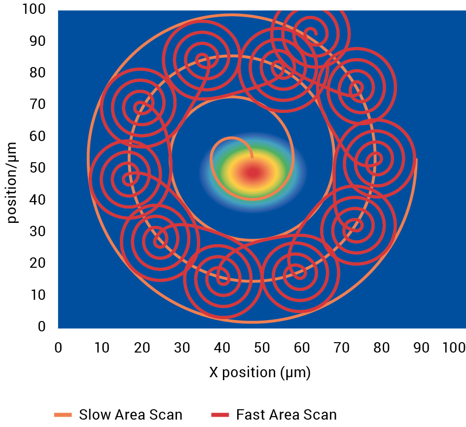
Figure 4b. Spiral scan using a hexapod/piezo approach. A fine and coarse scan can be executed simultaneously. Image Credit: PI (Physik Instrumente) LP
Gradient Searches
Gradient searches use a modest, roughly circular dither motion between devices to vary the coupling. This variation in the figure of merit enables the local gradient of the coupling to be determined in real time. The controller automatically detects modulation and directs the alignment to minimize it until it reaches zero, signaling complete optimization.
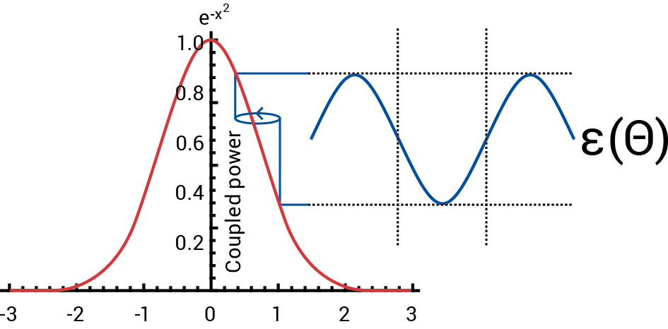
Figure 5. Graphical depiction of gradient determination via a circular dither, which modulates the observed coupled power (or other parameters). The modulation phase with respect to the dither indicates the direction towards maximum while its amplitude falls to zero when optimized. Image Credit: PI (Physik Instrumente) LP
|ε(Θ)| = ∇I = (Imin−Imax)/Imin
Figure 6. The observed gradient can be expressed by the above equation and serves as a measure of alignment error. Image Credit: PI (Physik Instrumente) LP
The controller can automatically calculate the local gradient based on the observed modulation (Figure 6).
The gradient (∇I) decreases to zero when optimized. Any axes in an FMPA system can execute various types of alignments, depending on their physical capabilities. Gradient searches are fast and precise methods for transverse optimization, but they can also be used for other purposes, such as:
- In a single linear axis, which is ideal for localizing the beam waist in a lens coupling
- In a gimbaling or swivelling fashion to optimize an angular orientation
- In a rotation about one channel axis of a multichannel device, to bring all elements of the device’s arrayed input/output (I/O) channels into correspondence
These techniques are suited for a wide range of optimizations, including bulk optic, cavity, and pinhole alignments.
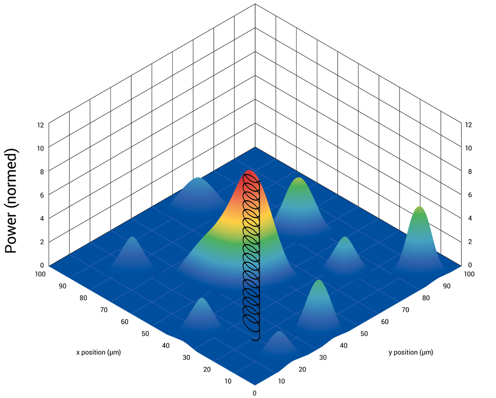
Figure 7. A graphical depiction of a digital gradient search (hill-climb algorithm). Once the main mode has been identified through an area scan, the algorithm will reach the peak quickly. The main peak is automatically fine-tuned in all DOF the application requires. All of this is achieved in parallel with one command by the user. With today’s photonic devices, it cannot be assumed that the peak is symmetrical, follows a Gaussian distribution, or has a circular cross-section. Furthermore, both edge and diffractive-coupler scenarios must be met. Image Credit: PI (Physik Instrumente) LP
Compensating for Position Changes
Photonic devices in packaging must be permanently bonded and attached to fibers to transfer signals, which is commonly accomplished with a UV-curing epoxy glue. However, polymerization happens during the curing process, which increases stress and causes component displacement.
As a result, a tracking mode within the FMPA algorithm is useful for correcting for positional changes in the optical elements in real time, during the early phases of polymerization, making the necessary corrections, and fine-tuning the alignment to maintain optimal orientation.
Solving the First Light Problem
Before the optimization steps can begin, an optical signal above the noise level must be detectable.
This procedure is known as first light detection. Finding first light has been time-consuming in all industrial photonics alignment applications, including wafer probing and device packing. It is especially difficult in devices with inputs and outputs since both sides must be aligned to provide even a minimal level of coupling.
Traditional First Light Search Algorithms
At the micron to submicron scale, cyclic patterns such as Archimedean spirals or sinusoidal raster scans are commonly used to detect signals (see Figures 4a and 4b).
In the case of considerable device-to-device variances or indeterminate fixturing, these repetitive, narrowly spaced scans might take a long time to complete, depending on parameters such as the area to be scanned, whether inputs and outputs must be aligned at the same time, and so on.
New First Light Capture Process
A unique, embedded search and alignment algorithm (patent pending) has been developed, potentially revolutionizing the area. The algorithm, known as PILightning, is integrated in PI's advanced controllers.
It enables highly dynamic mechanics, such as piezo scanners or direct-drive air bearing stages, to realize significant cost benefits over earlier first light search algorithms. This new procedure is completely automated and almost instantaneous, eliminating the need for extensive calibration or operator involvement.
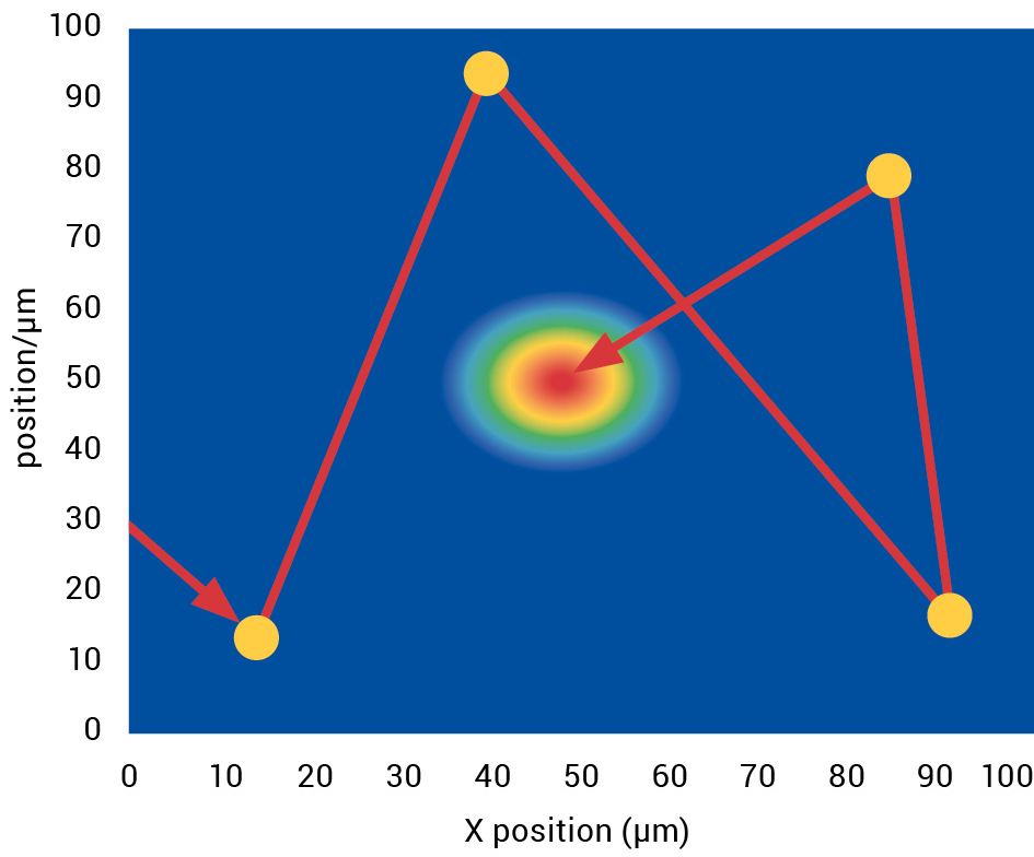
Figure 8. First light detection with PILightning. Learn more here. Image Credit: PI (Physik Instrumente) LP
PILightning is based on a novel search strategy that incorporates an AI-powered real-time executive function (Figure 8). It significantly decreases the time required to locate first light in single and double-sided couplings, as well as loopback (omega) waveguide arrangements.
Once the first light is detected, the FMPA (Fast Multi-Channel Photonics Alignment) fast gradient search method is activated, which uses real-time feedback control to rapidly optimize the alignment across degrees of freedom and channels.
Depending on the application, a tracking algorithm can be enabled to preserve optimal coupling efficiency, which is critical in curing circumstances.
Orders of Magnitude Improvement
PILightning has been shown in tests to minimize first light capture by an order of magnitude or more in single-sided alignment applications.
Double-sided applications yield gains that exceed two orders of magnitude. The broader the search area and (as with the FMPA parallel optimization functionality) the more complicated the alignment, the greater the benefit.
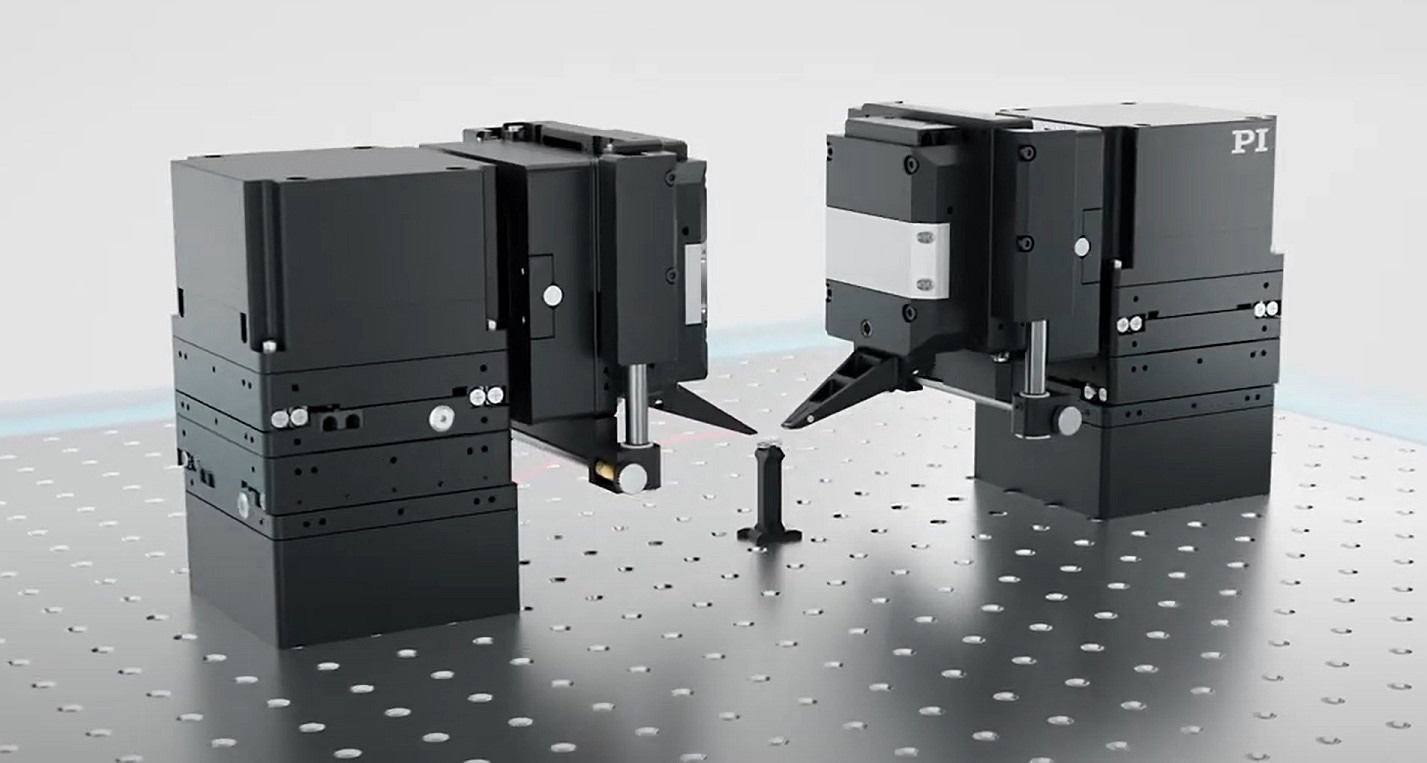
Figure 9. The F-141, dual-sided, PILightning-enabled fiber alignment system - dubbed PINovAlign - is designed to provide highest performance with the most compact footprint. It is available in 3-, 4-, and 6-axis configurations and provides exceptional throughput advantages in in fiber-array applications. Image Credit: PI (Physik Instrumente) LP
Mechanisms for Different Requirements
While the techniques outlined above apply to all types of mechanical alignment devices, differing requirements for alignment mechanisms, such as size, travel range, DOF, and so on, necessitate distinct configurations and technologies.
Optical Power Meters: Bandwidth and Dynamic Range Rule
A very sensitive power meter with a broad dynamic range and high bandwidth is also required to ensure the correct alignment of SiPh components. To fully utilize the FMPA algorithms, a signal bandwidth of 20 kHz and a dynamic range of six orders of magnitude with logarithmic output are typically used.
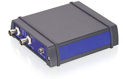
Figure 10. High-speed optical alignments require optical power meters with high bandwidths. Image Credit: PI (Physik Instrumente) LP
Gantry Platforms for Large Format Applications
Processing densely packed nanoscale structures over wide areas for a variety of applications, including semiconductor and SiPh testing and manufacture on circuit boards, trays, carriers, and other large substrates, necessitates high-accuracy, high-throughput solutions offered on dependable platforms.
Novel gantry systems are ideal for these applications since they greatly boost throughput while also delivering repeatable and resilient outcomes in a compact form factor.
Some current gantry systems, such as those offered by PI, employ power-dense ironless linear motors to handle the high dynamics necessary in photonics applications.
These efficient direct drive motors can include two high-resolution linear encoders on each gantry axis, with nanoscale or sub-nanometer resolutions, allowing for repeatable positioning even during the most demanding duty cycles.
Mechanical or air bearings are available, with the latter offering numerous benefits, including cleaner operation with no chance of contamination that could harm the delicate optical circuits. Controllers with and without built-in FMPA capabilities are available.
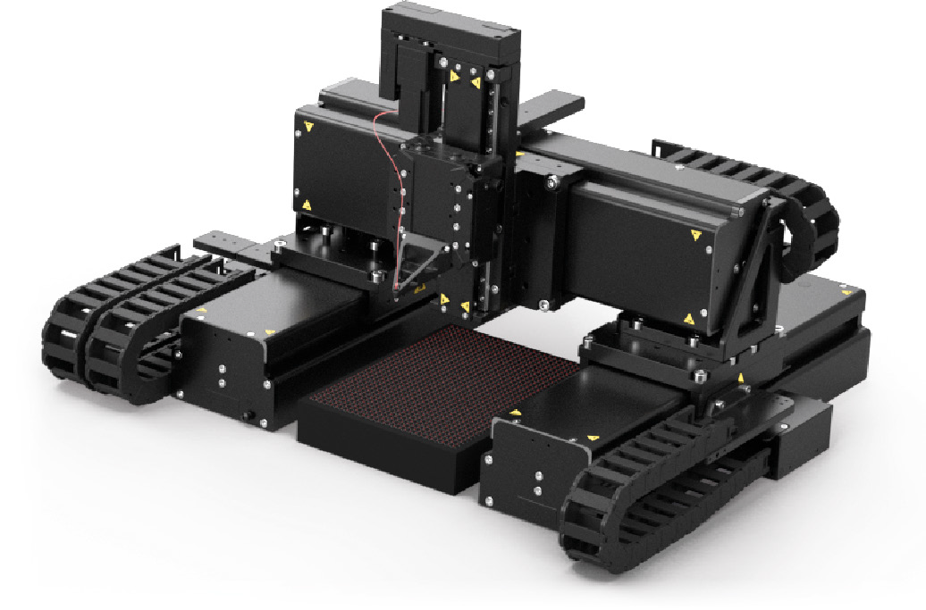
Figure 11. Mini Gantry. Image Credit: PI (Physik Instrumente) LP

This information has been sourced, reviewed and adapted from materials provided by PI (Physik Instrumente) LP.
For more information on this source, please visit PI (Physik Instrumente) LP.