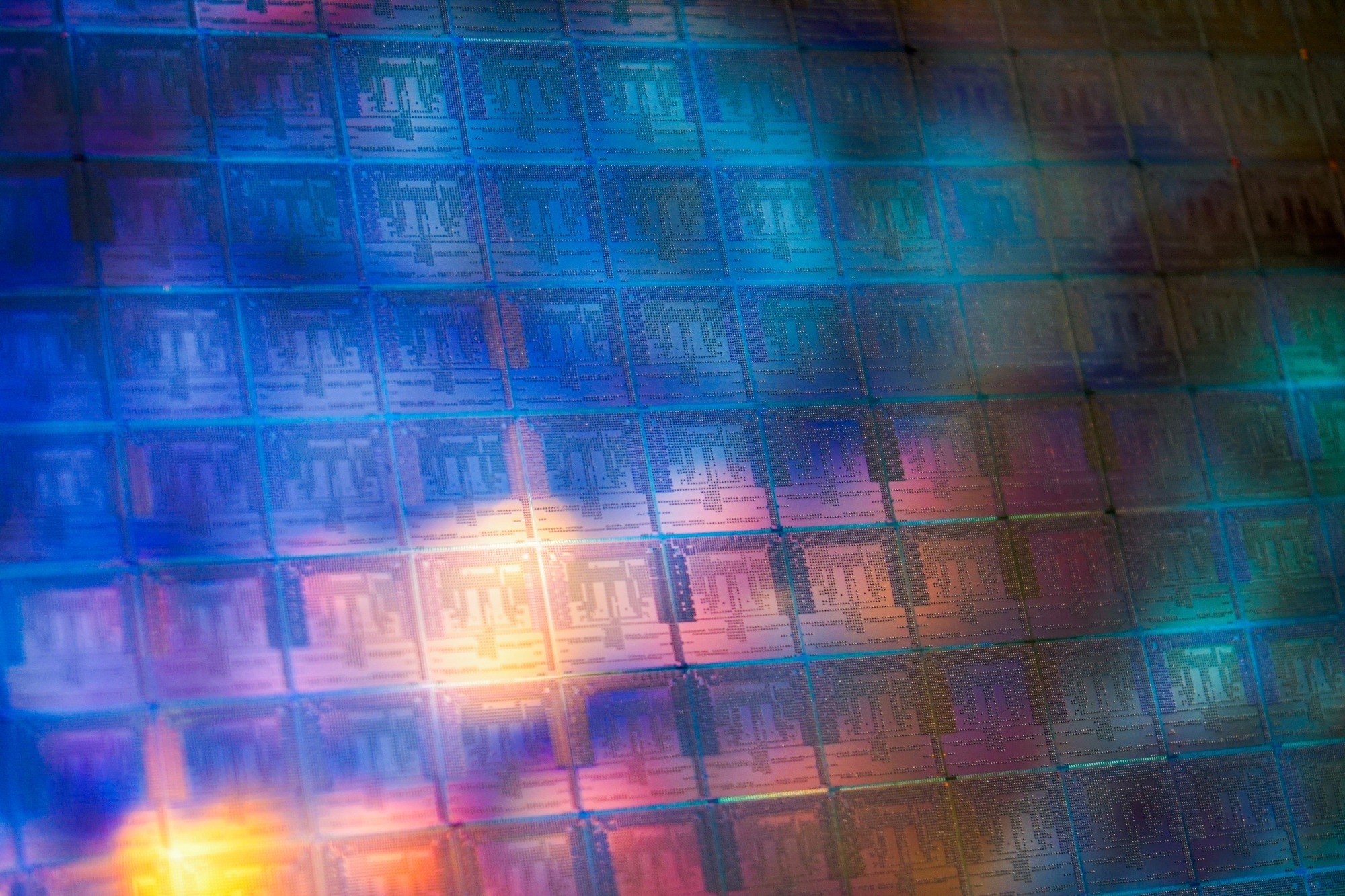
In a recent Nature article, researchers unveiled an ultralow-loss photonic integrated circuit (PIC) platform built with germano-silicate, a material widely recognized for its high performance in optical fibers,now manufactured using a fully CMOS-foundry-compatible process.

Image Credit: Sergey Saulyak/Shutterstock.com
Background
At shorter wavelengths (400–1,100 nm), waveguide losses fundamentally increase due to two primary factors. First, scattering losses become more pronounced as the optical wavelength approaches the scale of surface roughness, a phenomenon known as surface Rayleigh scattering. Second, absorption losses rise as photon energy enters the Urbach tail of amorphous or crystalline dielectric materials. Despite these challenges, numerous critical photonic applications, such as optical clocks, quantum computing, bioimaging, compact lidar, and atomic physics studies, rely on these shorter wavelengths. Silica and germanium-doped silica (germano-silicate) are extensively used in optical fibers for short-wavelength operation because of their extraordinarily low material absorption. However, utilizing these materials in a planar integrated photonic circuit has been hindered, either due to the necessity of suspended geometries for pure silica or the lack of mature fabrication processes for germano-silicate.
The Current Study
The fabrication process for the germano-silicate photonic integrated circuits (PICs) is carefully designed to be fully CMOS-compatible. It starts with depositing a 4-μm-thick germano-silica layer, containing 25 mol% GeO2, which results in approximately a 2% refractive index contrast, onto a 15-μm-thick thermal oxide layer on a silicon wafer. This is done using plasma-enhanced chemical vapor deposition (PECVD) at around 270?°C, a relatively low temperature that defines an anneal-free thermal budget for the entire process.
Ridge waveguides are then patterned in the germano-silica layer using a combination of ruthenium (Ru) and silica hard masks, deep-ultraviolet (DUV) lithography, and inductively coupled plasma (ICP) etching. The Ru mask plays a key role here, offering the high etch selectivity needed for fluorine-based deep etching of the Ge:silica material.
To reduce roughness-induced scattering losses and achieve ultrahigh Q factors across a wide spectral range, the wafer typically undergoes a furnace annealing step. This step causes the Ge-silica waveguide sidewalls to reflow, smoothing out etch-induced roughness, while the underlying thermally grown oxide (THOX) remains unaffected.
An optional upper cladding layer can be added post-annealing. Two cladding options were evaluated: a 14-μm-thick phosphorus-doped silica layer for full acoustic confinement, or a higher-quality ICP-PECVD silica cladding (exceeding 6?μm) to better shield the devices from long-term atmospheric exposure.
The use of DUV-stepper lithography throughout ensures high-precision patterning, which is essential for accurate dispersion engineering and device performance.
Results and Discussion
The germano-silicate PICs demonstrate record-low waveguide propagation losses spanning the violet to telecom bands. Resonator Q factors exceed 180 million across this wide spectrum, reaching a maximum Q of 463 million at 1,064 nm, which translates to a waveguide loss of 0.08 dB m−1. This lowest loss figure is comparable to the earliest low-loss optical fiber produced in 1970. Critically, the platform breaks the short-wavelength limitation, achieving a loss of 0.49 dB m−1 at 458 nm, representing a 13-dB improvement over previous records in the visible and short-NIR ranges.
Beyond loss performance, the platform’s material and structural advantages are demonstrated. Dispersion engineering, facilitated by the DUV-stepper-defined waveguides, enabled soliton microcomb generation. The material also facilitates acoustic mode confinement, which was verified through characterization of the stimulated Brillouin scattering (SBS) gain spectrum. Integrated germano-silicate resonators were used to create a high-coherence Brillouin laser, exhibiting a lasing frequency shift of 9.68 GHz, which is lower than the typical 10.9 GHz observed in standard silica resonators. This synergy of ultralow optical loss and engineered acoustic confinement enables low-noise Brillouin lasers for advanced gyroscopes and integrated microwave photonics.
Furthermore, the platform's large mode area (LMA) enhances hybrid-integrated low-noise lasers. Self-injection locking (SIL) of semiconductor diode lasers with ultrahigh-Q germano-silicate microresonators significantly reduces frequency noise. The large mode area, calculated at 28.06 μm2 for Ge-silica compared to 7.71 μm2 and 1.33 μm2 for thin and thick Si3N4, respectively, greatly suppresses thermal refractive noise (TRN). As a result, a commercial DFB laser coupled with a Ge-silica resonator achieved a Hz-level fundamental linewidth, corresponding to a 46-dB noise reduction relative to the free-running laser. Extending this into the visible spectrum, SIL of commercial Fabry–Pérot diode lasers resulted in fundamental linewidths of 15 Hz at 632 nm, 12 Hz at 512 nm, and 90 Hz at 444 nm.
Conclusion
In summary, the developed germano-silicate ultralow-loss platform substantially advances integrated photonics, achieving a >10 dB improvement in quality factor in both the violet wavelength range and for anneal-free processing. The platform also features readily engineered dispersion, acoustic mode confinement, and thermal stability, demonstrated through soliton microcomb generation, stimulated Brillouin lasing, and low-frequency-noise self-injection locking. Crucially, ultralow losses are achieved without post-processing thermal annealing in the telecom band, offering a 10-fold reduction in anneal-free waveguide loss over previous records and enabling easier heterogeneous integration. The success of this germano-silicate platform can enable fiber-like loss on a chip and bridge ultralow-loss technology to applications like optical clocks and quantum sensors.
Download the PDF of this page
Source:
Journal Reference
Chen H. J., Colburn K., et al. (2026). Towards fibre-like loss for photonic integration from violet to near-infrared. Nature 649, 338–344. DOI: 10.1038/s41586-025-09889-w, https://www.nature.com/articles/s41586-025-09889-w