Reviewed by Frances BriggsNov 25 2025Reviewed
ETH Zurich’s OLED innovation reshapes what's possible in screens, microscopes, and optical computing with its nanoscopic pixels.
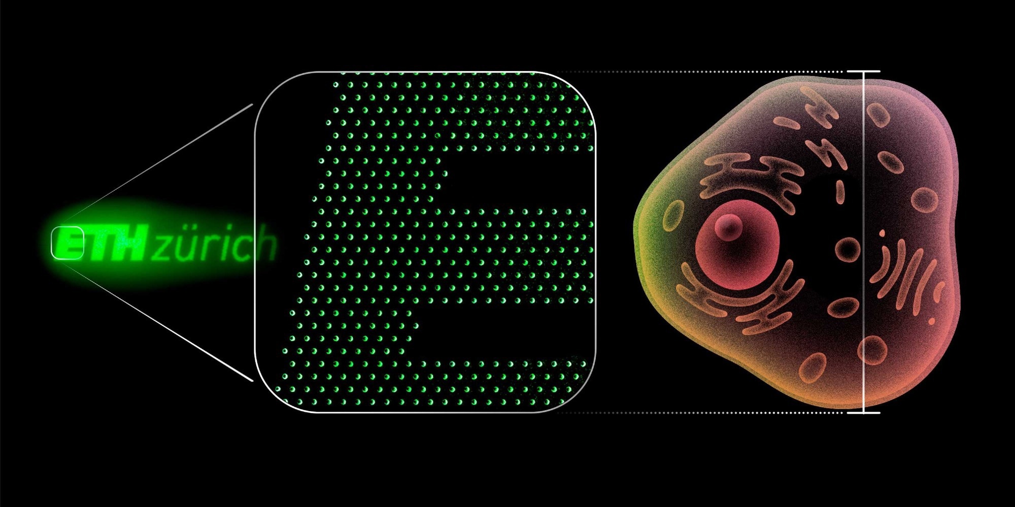 This ETH Zurich logo consists of 2,800 nano light-emitting diodes and, at a height of 20 µm, matches the size of a human cell. A single pixel measures around 0.2 micrometers (200 nm). Image Credit: Amanda Paganini / ETH Zurich
Researchers at ETH Zurich have successfully manufactured organic light-emitting diodes (OLEDs) at the nanoscale, achieving dimensions approximately one hundred times smaller than a human cell.
This significant advancement not only facilitates the development of ultra-high-resolution screens and advanced microscopy systems but also, critically, opens up entirely novel possibilities for wave optics applications due to the extremely minute pixel size inherent in these devices.
The study was detailed in Nature Photonics.
The semiconductor industry's fundamental progress is driven by miniaturization, a principle that has enabled significant gains in computer performance since the 1950s through the fabrication of increasingly smaller structures on silicon chips.
Chemical engineers at ETH Zurich have recently extended this trend by achieving a reduction in the size of organic light-emitting diodes (OLEDs) by several orders of magnitude. This development is relevant to OLEDs currently used in premium mobile phones and TV screens.
Miniaturized in One Single Step
Light-emitting diodes (LEDs) are semiconductor-based electronic components designed to convert electrical current into light.
The diameter of the most minute OLED pixels we have developed to date is in the range of 100 nanometers, which means they are around 50 times smaller than the current state of the art.
Jiwoo Oh, Doctoral Student, Nanomaterial Engineering Research Group, ETH Zurich
The research group is headed by ETH Professor Chih-Jen Shih. The manufacturing process for these novel nano-OLEDs was co-developed by Oh and Tommaso Marcato.
In just one single step, the maximum pixel density is now around 2500 times greater than before.
Tommaso Marcato, Postdoc, ETH Zurich
For context, the miniaturization rate of computer processors historically adhered to Moore's Law until the 2000s, dictating a doubling of electronic element density approximately every two years.
Screens, Microscopes, and Sensors
These newly developed pixels, ranging from 100 to 200 nm, lay the foundation for ultra-high-resolution displays, potentially enabling razor-sharp imagery in near-eye applications, such as smart glasses.
To demonstrate this capability, Shih's research team fabricated an ETH Zurich logo comprising 2,800 nano-OLEDs. This logo, comparable in size to a human cell, features individual pixels approximately 200 nm (0.2 µm) in dimension. The current minimum pixel size achieved by the ETH Zurich researchers is 100 nm.
These minute light sources offer significant utility in high-resolution microscopy, facilitating precise focusing within the sub-micrometer range.
“A nano-pixel array as a light source could illuminate the most minute areas of a sample – the individual images could then be assembled on a computer to deliver an extremely detailed image,” explained the professor of technical chemistry.
Nano-pixels could even be used as miniature sensors, with potential applications in detecting signals from individual nerve cells.
Nano-Pixels Generating Optical Wave Effects
These minute dimensions also open up possibilities for research and technology that were previously entirely out of reach, a point Marcato emphasizes.
When two light waves of the same color converge closer than half their wavelength – the so-called diffraction limit – they no longer oscillate independently of each other, but begin to interact with each other.
Tommaso Marcato, Postdoc, ETH Zurich
The fundamental diffraction limit for visible light, which typically ranges between 200 and 400 nanometers depending on the specific wavelength, dictates the minimum achievable feature size in optical systems. Significantly, the nano-OLED technology developed by ETH researchers demonstrates the capability to achieve pixel spacing within this critical proximity.
The foundational principle of wave interaction is effectively demonstrated by the interference patterns generated when two disturbances, such as stones dropped into a calm water body, create overlapping circular waves.
The resulting superposition manifests as a distinct geometric arrangement of reinforced crests and attenuated troughs.
Extending this principle, intelligently configured nano-OLED arrays are capable of generating sophisticated optical wave effects. This enables the precise manipulation of light, where emissions from adjacent pixels can be engineered for mutual constructive reinforcement or destructive cancellation.
Manipulating Light Direction and Polarization
Through their initial experimental work, Shih's team successfully harnessed specific interactions to control the direction of emitted light precisely.
This breakthrough allows the OLEDs to project light exclusively at highly specific angles, a significant departure from the previous omnidirectional emission across the chip's surface.
“In the future, it will also be possible to bundle the light from a nano-OLED matrix in one direction and harness it to construct powerful mini lasers,” said Marcato.
The generation of polarized light, characterized by oscillations confined to a single plane, has been demonstrated by researchers through specific interaction mechanisms. This capability is currently leveraged in medical applications, for instance, to distinguish between healthy and cancerous tissues.
The significant potential of these interaction-based principles is well-illustrated by modern radio and radar technologies. These systems, which operate across wavelengths ranging from mm to km, have long exploited such interactions.
Phased array arrangements, in particular, encourage the precise alignment and focusing of antennas and transmitted signals.
Applying these technological advancements within the optical spectrum could yield substantial benefits, including the further acceleration of information transmission in data networks and computers.
Ceramic Membranes Making All the Difference
In the current production of OLEDs, light-emitting molecules are vapor-deposited onto silicon chips. This process uses relatively thick metal masks, resulting in larger pixels.
As Oh explains, the push for miniaturization is now possible through a unique ceramic material.
“Silicon nitride can form very thin yet resilient membranes that do not sag on surfaces measuring just a few square mm,” said Oh.
The outcome was the production of nano-OLED pixel placement templates, demonstrating a thickness approximately 3,000 times smaller.
Our method also has the advantage that it can be integrated directly into standard lithography processes for the production of computer chips.
Jiwoo Oh, Doctoral Student, Nanomaterial Engineering Research Group, ETH Zurich
Opening a Door to Novel Technologies
The researchers are now optimizing the methodology. This optimization encompasses not only the further miniaturization of the pixels but also the development of effective control mechanisms.
“Our aim is to connect the OLEDs in such a way that we can control them individually,” said Shih.
Optimizing the interactions between light pixels is fundamental to realizing their full potential. This requires the development of precisely controllable nano-pixels, which are poised to enable novel applications within phased array optics – a technology renowned for its capacity to steer and focus light waves electronically.
Historically, the 1990s saw the postulation that phased array optics could facilitate holographic projections from two-dimensional screens.
However, current research, spearheaded by Shih, envisions a more advanced concept: the future integration of interacting OLED groups into spatially precise meta-pixels.
“This would allow 3D images to be realized around viewers,” said the chemist.
Journal Reference:
Marcato, T., et al. (2025) Scalable nanopatterning of organic light-emitting diodes beyond the diffraction limit. Nature Photonics. DOI:10.1038/s41566-025-01785-z. https://www.nature.com/articles/s41566-025-01785-z