Nov 9 2011
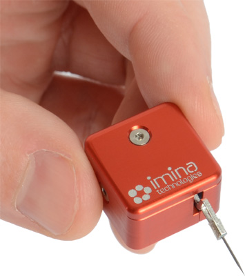
What is the size of a gambling die, zips around a microscope stage at 2mm/s but can stop on a dime with nanometer precision, then manipulate and probe anything from biological cells to semiconductors, MEMs or LEDs? They are the new “miBots” from Imina Technologies (Ecublens, Switzerland).
miBots are more than nanomanipulators. Unlike conventional systems, they are virtually untethered and move independently. Working individually or in groups, they can be fitted with a variety of tools such as grippers, probes, and optical fibers so that, in addition to manipulating the sample, they can illuminate a nano workspace and conduct force or electrical measurements. Vacuum ready, miBots’ proprietary monolithic structure makes them robust, mechanically and thermally stable, and less sensitive to vibration.
Driven by piezo actuators, miBots scoot around the microscope stage, pivot, and lift their tools up and down, all at the touch of a joystick or easy-to-use graphical interface. These intuitive human interfaces make miBots easy to set up and easy to learn, reducing time and eliminating the risk of sample damage. Their independent X, Y, and Z controls deliver the delicate positioning especially important in scanning electron microscopy (SEM) where limited depth of focus makes maneuvering a challenge. For increased productivity and time savings, miBots can be programmed to do repetitive tasks using scripting languages like MATLAB®.
Imina Technologies has engineered a variety of stage options for these novel mini robots. For conventional installation on inverted light microscopes (LM), SEMs, or focused-ion beam systems (FIBs), the “miBase” provides control and maneuvering room for up to four miBots. Special apertures accommodate illumination for the LM and stubs for SEMs, and multiple coaxial I/O connections enable electrical characterization and testing.
For custom applications or smaller SEMs, the “miCube” and “multiCube” provide bases for one or four miBots, respectively, while for large samples such as semiconductor wafers, the new “XY-13-OL” platform offers 13x13mm travel with 50nm precision. Installation for each of the stages is straightforward, requiring minimal technical expertise. A turnkey vacuum kit facilitates installation inside any electron microscope.
miBots will be working in the Imina Technologies booth at the upcoming Materials Research Society Fall Meeting (Booth #1304, Nov 28-Dec 2, Boston, MA.,MRS.org), and at a series of West Coast workshops (Dec 5-9). For workshop details and videos of the miBots in action, visit www.imina.ch.