A team of researchers from the University of Illinois have successfully demonstrated an optoelectronically active three-dimensional photonic crystal. The research findings have been published by the team in the Journal, Nature Materials.
The lead researcher and professor of material science and engineering, Dr Paul Braun stated that the team was able to generate new optical properties in a semiconductor material by changing the three-dimensional structure at the same time maintaining the electrical properties of the material.
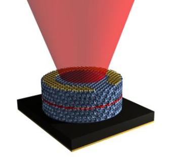 The 3D photonic crsytal LED developed by researchers at the University of Illinois
Unlike traditional optical devices and materials, photonic crystals have unique physical structures that allow the material to control/manipulate light by inducing a typical phenomena, thus affecting the behavior of photons. This property of photonic crystals makes them popular study materials for applications in solar energy, lasers, metamaterials and LEDs.
Earlier attempts at creating three-dimensional photonic crystals resulted in optically active devices capable of directing light but incapable of turning electricity to light. The photonic crystal created by the research team at the University of Illinois has both the desired properties.
During the creation process of the three-dimensional optoelectronic photonic crystal, the researchers deposited semiconductor gallium arsenide (GaAs) within the gaps of a template packed with tiny spheres. The semiconductor grows as a single unit crystal from the base up, an industrial process called epitaxy. After the template fills up, the spheres are removed, thus leaving a porous three-dimensional single-crystal semiconductor structure. The researchers then cover the structure with a thin film of semiconductor with a broader bandgap in order to stop surface recombination and improve its performance.
The researchers built a three-dimensional LED photonic crystal to test the technique. The researchers inferred that by utilizing different semiconductor materials or by altering the structure, solar collection could be improved or specific wavelengths could be targeted for low-threshold lasers or metamaterials applications.