May 20 2010
Palomar Technologies, a world leader in providing solutions for microelectronic and optoelectronic packaging, and experts in precision wire bonding, complex hybrid packaging, and high accuracy die bonding systems, announced today that it will exhibit at the MicroElectronics Packaging and Test Engineering Council (MEPTEC) Symposium held in San Jose, May 20, 2010.
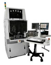 6500 Ultra High Accuracy Die Bonder
Palomar Microelectronics, the development, test, and contract assembly division of Palomar Technologies, has recently done several successful wafer scale optical sub-assemblies for applications in the high tech consumer market. As an emerging market, many participating companies are start-ups and often cash-strapped when it comes to making a large equipment purchase. Palomar Microelectronics' contract assembly is an ideal solution.
With wafer scale optical sub-assemblies, the bonding is done directly to the wafer. High accuracy is important in this process: +/- 1.5 - 5 microns allows for passive alignment, which eliminates expensive active alignment processes. An example of an "optical sub-assembly" is eutectic and epoxy LASER, LED another components such as photo-detectors and lenses. Some of these sub-assemblies require encapsulation. For example, an LED may require coating for a selective wavelength and some circuits require protection for the wire bonds.
The beauty of wafer scale packaging is that it enables the user to have more scalable production via the use of the wafer's nearly 3,000 sites - each site is a package. Palomar bonders are designed for large area and deep access, allowing the operator to position a wide variety of wafers and substrates, up to 300mm square (requiring 180 degree rotation), on the bonding system.
Palomar's 6500 Ultra High Accuracy Die Bonder has a special configuration for Wafer Scale Packaging, designed for high speed, precision P-Side Down Laser Die to Wafer Eutectic Assembly. Applications include P-Side Down Laser Diode Attachment (Die to Wafer) and Pulsed Heat Pick Tool for 80/20 Au/Sn pulsed reflow attachment.