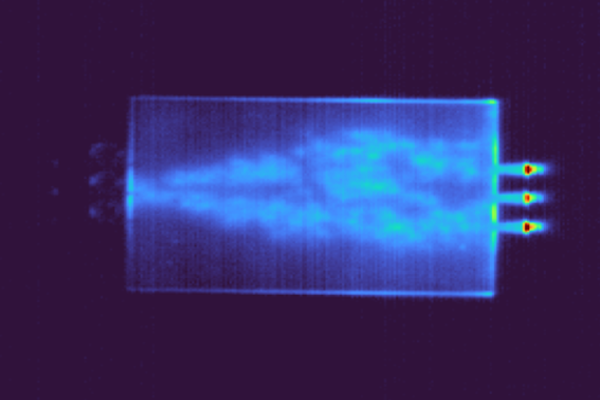
Light creates a computational network on a piece of unpatterned semiconductor wafer. The Feng Lab team’s achievement allows for on-chip processing with no lithographic etching, signaling cheaper and easier manufacturing and superior accuracy for AI applications. Image Credit: University of Pennsylvania School of Engineering and Applied Science
As well as their incredible speed, photonic circuits make use of considerably less energy than electronic ones.
The motion of electrons is comparatively slow via hardware, thereby colliding with other particles and producing heat, while photons flow without losing energy, producing no heat.
Electronics and photonics draw on isolated areas of science and make use of diverse architectural structures. However, both depend on lithography to specify their circuit elements and sequentially link them.
While photonic chips fail to make use of the transistors that inhabit electronic chips’ ever-shrinking and layered grooves, their complicated lithographic patterning guides laser beams via a coherent circuit to develop a photonic network that could make computational algorithms to be executed.
Now for the first time, scientists at the University of Pennsylvania School of Engineering and Applied Science have made a photonic device that offers programmable on-chip information processing in the absence of lithography. This helps provide the speed of photonics augmented by excellent flexibility and precision for AI applications.
Obtaining peerless control of light, this device comprises spatially distributed optical gain and loss. Lasers cast light instantly on a semiconductor wafer without the need for specified lithographic pathways.
Liang Feng, Professor in the Departments of Materials Science and Engineering (MSE) and Electrical Systems and Engineering (ESE), together with Ph.D. student Tianwei Wu (MSE) and postdoctoral fellows Zihe Gao and Marco Menarini (ESE), introduced the microchip in a recent study reported in the Nature Photonics journal.
The computational landscape has been changed as a result of silicon-based electronic systems. However, they have clear limitations: they are slow in processing signals, they work via data serially and not in a parallel manner, and they can only be miniaturized to some extent. Photonics is considered to be one of the most hopeful alternatives since it has the potential to overcome all these drawbacks.
But photonic chips intended for machine learning applications face the obstacles of an intricate fabrication process where lithographic patterning is fixed, limited in reprogrammability, subject to error or damage and expensive.
Liang Feng, Professor, Departments of Materials Science and Engineering and Electrical Systems and Engineering, University of Pennsylvania School of Engineering and Applied Science
Feng added, “By removing the need for lithography, we are creating a new paradigm. Our chip overcomes those obstacles and offers improved accuracy and ultimate reconfigurability given the elimination of all kinds of constraints from predefined features.”
These chips have turned out to be adaptable data-processing powerhouses without lithography. This is because the patterns are not pre-defined and etched in, and the device is free of defects in an intrinsic manner. Probably, the lack of lithography makes the microchip impressively reprogrammable, able to customize its laser-cast patterns for utmost performance, be the task simple (few inputs, small datasets) or complicated (many inputs, large datasets).
Put differently, the minimalism or intricacy of the device is a sort of living thing, adaptable in methods that no etched microchip could be.
What we have here is something incredibly simple. We can build and use it very quickly. We can integrate it easily with classical electronics. And we can reprogram it, changing the laser patterns on the fly to achieve real-time reconfigurable computing for on-chip training of an AI network.
Tianwei Wu, Ph.D. Student, University of Pennsylvania School of Engineering and Applied Science
A modest slab of semiconductor, the device could not be simpler. It is the manipulation of the material properties of the slab which is the key to the research team’s innovation in projecting lasers into dynamically programmable patterns to reconfigure the computing functions of the photonic information processor.
This eventual reconfigurability is considered vital for AI and real-time machine learning.
The interesting part is how we are controlling the light. Conventional photonic chips are technologies based on passive material, meaning its material scatters light, bouncing it back and forth. Our material is active. The beam of pumping light modifies the material such that when the signal beam arrives, it can release energy and increase the amplitude of signals.
Marco Menarini, Postdoctoral Fellow, University of Pennsylvania School of Engineering and Applied Science
Gao added, “This active nature is the key to this science, and the solution required to achieve our lithography-free technology. We can use it to reroute optical signals and program optical information processing on-chip.”
Feng makes a comparison of the technology to an artistic tool, a pen for drawing pictures on a blank page.
Gao stated, “What we have achieved is exactly the same: pumping light is our pen to draw the photonic computational network (the picture) on a piece of unpatterned semiconductor wafer (the blank page).”
But unlike indelible lines of ink, such beams of light could be drawn and redrawn, their patterns tracing countless paths to the future.
Journal Reference:
Wu, T., et al. (2023) Lithography-free reconfigurable integrated photonic processor. Nature Photonics. doi.org/10.1038/s41566-023-01205-0.