MEMS technology could enable more efficient fiber-optical telecommunications, datacenters, and future quantum computers. Image Credit: Professor Niels Quack, University of Sydney
According to Associate Professor Quack from the School of Aerospace, Mechanical, and Mechatronic Engineering, photonic MEMS are special because they are quick, support a wide variety of optical carrier signals, are small, require very little power, and have minimal optical loss.
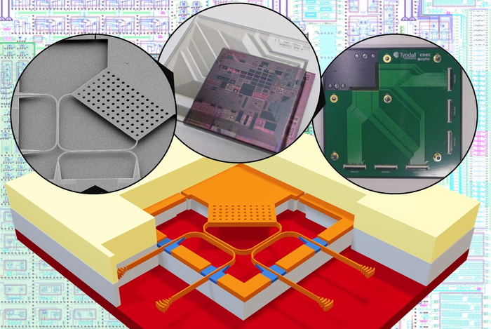
This is the first time that nano-electro-mechanical actuators have been integrated in a standard silicon photonics technology platform. It is an important step towards mature large-scale, reliable photonic circuits with integrated MEMS. This technology is being prepared for high-volume production, with potential applications in 3D imaging for autonomous vehicles or new photonic assisted computing.
Niels Quack, Assistant Professor, School of Aerospace, Mechanical, and Mechatronic Engineering, University of Sydney
He added, “Current similar technologies consume a lot of power and occupy a large area on-chip. They also have high optical losses. This makes the integration of a large number of components on a single chip challenging. Our silicon photonic MEMS technology overcomes these shortcomings, providing a route for efficient scaling of photonic integrated circuits.”
“The technology will advance knowledge in the field of micro- and nanofabrication, photonics, and semiconductors, with a wide range of applications. These include beam steering for LIDAR 3D sensing in autonomous vehicles, programmable photonic chips, or information processing in quantum photonics,” Quack concluded.
Declaration
The authors assert they have no conflicting interests. The European Union has funded this work as part of the MORPHIC H2020 project under grant number 780283. N.Q. expressed gratitude to the Swiss National Science Foundation for financing it under grant 183717.
The work described in this manuscript was completed when N. Q. was at EPFL, and it was partially written while N. Q. was at the University of Sydney. The EPFL Center of MicroNanoTechnology (CMi) is gratefully acknowledged by the authors.
Journal Reference
Quack, N., et al. (2023) Integrated silicon photonic MEMS. Microsystems & Nanoengineering. doi:10.1038/s41378-023-00498-z.