Apr 23 2018
The electronic devices - such as smartphones, computers, and others - that we use in our everyday lives include billions of transistors, the fundamental building block invented in the late 1940s in Bell Labs. Initially, the size of the transistor was nearly 1 cm. However, advancement of technology has led to a considerable reduction in its size up to 14 nm, or 1000 times smaller than the width of a strand of human hair.
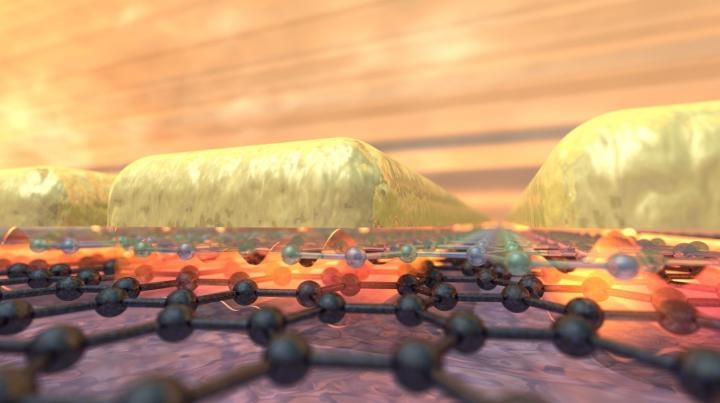 This is an artistic impression of the squeezed light (plasmon) in between the metal and graphene, separated by just one a one-atom-thick dielectric. (Image credit: ICFO)
Simultaneously, research is on to further reduce the size of the devices that control and guide light. Light can act as an ultra-fast communication channel, for instance, between distinctive sections of a computer chip; however, it can also be used in the case of innovative on-chip nanoscale lasers and ultra-sensitive sensors.
Innovative methods looking for ways to confine light into very tiny spaces, millions of times smaller than the prevalent ones, have been increasing. Earlier, scientists had discovered that metals have the ability to compress light below the wavelength scale (diffraction limit); however, more confinement would always lead to more energy losses. This scenario has now been changed through the use of graphene as an alternative.
According to a recent study reported in the Science journal, scientists from ICFO have been successful in achieving the utmost level of confinement of light. Precisely, they have been successful in confining light down to a space with dimensions of just one atom thick, the smallest confinement ever achieved. The study was headed by Frank Koppens, ICREA Professor at ICFO, and performed by David Alcaraz, Sebastien Nanot, Itai Epstein, Dmitri Efetov, Mark Lundeberg, Romain Parret, and Johann Osmond from ICFO, and carried out in collaboration with University of Minho (Portugal) and MIT (USA).
The research team used stacks, or heterostructures, of 2D materials to construct an entirely new nano-optical device, resembling an atom-scale Lego. They stacked a hexagonal boron nitride (hBN) monolayer (insulator) on a graphene monolayer (semi-metal), and on top of this, they deposited an array of metallic rods. Graphene was chosen for its ability to guide light in the form of “plasmons,” or oscillations of the electrons, which interact strongly with light.
They made infrared light to pass through their devices and observed the propagation of the plasmons in between the graphene and the metal. In order to get to the smallest possible space, they decided to reduce the gap between the graphene and the metal as much as possible to investigate whether the confinement of light stayed effective, for instance, without any additional loss of energy. Astonishingly, they observed that even though a hBN monolayer was used as a spacer, the plasmons were still excited by the light and were free to propagate when they were confined to a channel that is only one atom thick. They could switch the plasmon propagation on and off just through the application of an electrical voltage, thereby showing that light guided in channels with a height less than 1 nm could be controlled.
The outcomes of this study could lead to the development of an entirely innovative world of optoelectronic devices with a thickness of just 1 nm, such as ultra-small sensors, detectors, and optical switches. Owing to the exemplary shift in optical field confinement, exceptional interactions between light and matter, which could not be observed earlier, can now be investigated. The most exciting fact is that the atom-scale lego-toolbox of 2D materials has at present been also demonstrated to be applicable for different types of entirely new materials devices in which both electrons and light can be controlled even down to the scale of 1 nm.
The European Research Council, the European Graphene Flagship, the Government of Catalonia, Fundació Cellex, and the Severo Ochoa Excellence program of the Government of Spain partially supported this study.