3D-Micromac AG, a leading supplier of laser micromachining and roll-to-roll laser systems for the photovoltaic, medical device and electronics markets, today announced that its microDICE™ laser micromachining system has been adopted by a major industrial manufacturer for volume production of high-power diodes.
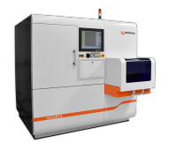 The microDICE™ laser micromachining system from 3D-Micromac supports volume production of high-power diodes.
Leveraging 3D-Micromac's proprietary TLS-Dicing™ technology, the microDICE system provides fast, clean and cost-effective dicing of wafers used for advanced semiconductors and power device applications. Its unique approach uses thermally induced mechanical stress to separate brittle semiconductor materials such as silicon, silicon carbide (SiC), germanium (Ge) and gallium arsenide (GaAs).
TLS-Dicing is a contact- and residue-free process that provides significantly higher throughput, higher yields and greater functionality compared to traditional die-separation technologies. For example, throughput is up to 30X greater compared to saw dicing. The technology also provides lower cost of ownership than other approaches. A forceless and contactless machining process, TLS-Dicing eliminates tool wear and requires no expensive consumables for surface cleaning—resulting in cost savings of up to an order of magnitude or more.
"While significant time and resources are invested in the front-end of semiconductor manufacturing to produce a completed product wafer, back-end wafer processing has historically been viewed as a necessary evil," stated Tino Petsch, CEO of 3D-Micromac. "That's all changed with the adoption of new types of wafer substrates, thinner wafers and scaling to smaller dimensions, larger-size substrates, and new packaging technologies like 3D-stacking. Back-end process steps such as wafer dicing are evolving as critical value-add process steps that not only ensure, but also further enhance, device yields. Using our TLS-Dicing technology, the microDICE system provides superior wafer dicing performance over other approaches while considerably reducing the dicing cost per wafer. Our technology has been proven in the photovoltaic and other industrial markets, and we are pleased to bring the benefits of it to the semiconductor and power device manufacturing industry."
3D-Micromac also announced today that it is expanding its global infrastructure with the opening of its new 3D-Micromac America headquarters in the heart of Silicon Valley, in San Jose, Calif. Serving as both an applications lab and sales and support facility, the office marks the company's first major presence in North America and will enable 3D-Micromac to better meet rising customer demand for its laser micromachining products across all of its served markets, including solar, semiconductor, MEMS, display and smart glass.