Jul 7 2016
A team of researchers from the Graphene Flagship have taken a crucial step to integrate graphene in silicon photonics. They have published a paper illustrating graphene’s ability to offer an uncomplicated solution for silicon photodetection in the telecommunication wavelengths. This innovative research was conducted as a collaboration project between the University of Cambridge (UK), John Hopkins University (USA), and The Hebrew University (Israel).
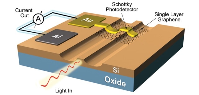 Graphene based Schottky Photodetector device. (Photo credit: Dr Ilya Goykhman, University of Cambridge, Cambridge Graphene Centre)
Graphene Flagship’s mission is to move graphene out of academic laboratories with the assistance from industry, and eventually into society. This highly ambitious goal plays a pivotal role in the choices made to guide the Flagship. The Flagship focuses on issues where it can make a lasting difference such as in Optical Communications.
Optical Communications are growing in importance as they have the ability to offer a solution to one of the greatest problems faced by the information age - energy consumption. All human actions in daily life consume information, and all of this information is possible as it is powered by energy. A demand for more information, would result in an increasing need for energy. In the near future, machine-to-machine communication and the Internet of Things (IoT) will be the major consumers of data traffic.
To enable the IoT and the level of information it needs, silicon photonics that exist today will have a problem. It will need ten times more energy than what is possible. So, to have this new optimized internet age, new technological, power-efficient solutions have to be developed. This is the reason why progress in graphene-based optical communication is vital.
The capability of the optical communications has increased when compared to standard metal-based electronic interconnects over the past few years. Silicon-based photo-detectors that are currently used in optical communications have a major flaw when locating data in the near infrared range, which is the range required for telecomminications. The telecom sector has been able to tackle this issue by incorporating germanium absorbers with the basic silicon photonic devices. Using this process, fully functioning devices on chips has been possible. But this is a complicated process.
In the latest study, highly responsive Schottky barrier photodetectors are produced by interfacing graphene with silicon on a chip. These graphene-based photodetectors are capable of 0.37 A/W responsivity at 1.55 μm using avalanche multiplication. This high responsivity can be compared to the responsitivity delivered by silicon germanium detectors presently used in silicon photonics.
From the Cambridge Graphene Centre, Professor Andrea Ferrari, who is also the Science and Technology Officer and the Chair of the Management Panel for the Graphene Flagship stated; “This is a significant result which proves that graphene can compete with the current state of the art by producing devices that can be made more simply, cheaply and work at different wavelengths. Thus paving the way for graphene integrated silicon photonics.”
Dr Ilya Goykhman, from the University of Cambridge, and the paper's lead author, said; “The vision here is for graphene to play an important part in enabling optical communication technologies. This is a first step towards this, and, over the next two years the aim of the wafer-scale integration and optoelectronics work-packages of the Flagship is to really make this happen”.
Graphene can beat current silicon photonic technology in terms of energy consumption. The Graphene Flagship is investing a lot of resources into wafer-scale integration with the creation of a new Work Package. We have identified a vision, where graphene is the backbone for data communication, and we plan to have a telecommunication bank capable of transferring 4x28 GB/s by 2018. The research in this Nano Letters paper is the first step towards achieving that vision, the importance of which is clearly recognized by companies such as Ericsson and Alcatel-Lucent who have joined the Flagship to help develop it. We have shown the potential for the detector but we also need to produce a graphene-based modulator to have a full, low energy optical telecommunication system and the Flagship is working hard on this problem. The Flagship has collected the right people in the right place at the right time to work together towards this goal. Europe will be at the cutting edge of this technology. It is a great challenge, and a great opportunity for Europe, as there is such high added value to the devices it will be cost effective to manufacture the device in Europe - keeping the value of the technology within the European community.
Professor Andrea Ferrari, Cambridge Graphene Centre