Researchers at three Fraunhofer Institutes have devised key components for EUV lithography.
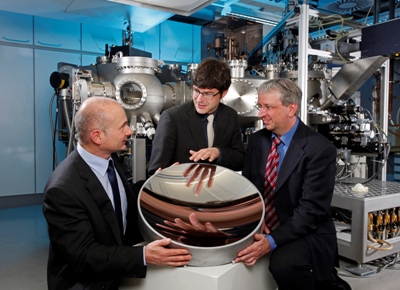 Jointly developed key components for EUV lithography: Dr. Torsten Feigl, Dr. Stefan Braun and Dr. Klaus Bergmann (from left to right) with a collector mirror. © Dirk Mahler / Fraunhofer
Dr. Klaus Bergmann’s team from the Fraunhofer Institute for Laser Technology has developed light sources, while Dr. Torsten Feigl’s team from the Fraunhofer Institute for Applied Optics and Precision Engineering has developed collector optics and Dr. Stefan Braun’s team from the Fraunhofer Institute for Material and Beam Technology has designed illumination and projection optics.
A 2012 Joseph-von-Fraunhofer prize will be awarded to the teams involved in this strategic collaboration for their remarkable achievements. Dr. Bergmann’s team designed the EUV source’s first prototypes in 2006. A beta version is already being utilized in industrial applications to expose chips. Bergmann informed that the fast, pulsed release of electrically stored energy is the basis of the concept. In the method, a laser was used to vaporize a trace quantity of tin, which was then agitated several times per second to an emission at 13.5 nm using a high current.
A collector mirror’s quality is the key to allow the radiation to hit the exposure mask in the right spot accurately. The coating ensures minimal losses and superior quality, focused EUV radiation. Dr. Feigl stated that the challenge faced by the team was to design a multilayer coating system with superior radiation stability, thermal stability and EUV reflectance and to apply it over a curved collector surface. The resultant system is a more than 660-mm-dia multi-layer coated EUV mirror, which is marked as the largest of its kind in the world.
Projection mirrors are used for exposing the radiation that passed the mask onto the chips. Dr. Braun’s team has developed the optimum reflection layer for the projection mirrors. Magnetron sputtering offers optimum layer accuracy without the need of in-situ thickness control or additional polishing processes.
The new EUV lithography system is anticipated to commence commercial production in 2015.