Recent computational advances, such as artificial intelligence (AI), have highlighted the limitations of current computing hardware employing electronic transistors and the von Neumann model. The inability of Moore’s law to further scale very large-scale integration (VLSI) technology has increased the demand for novel computing devices.1
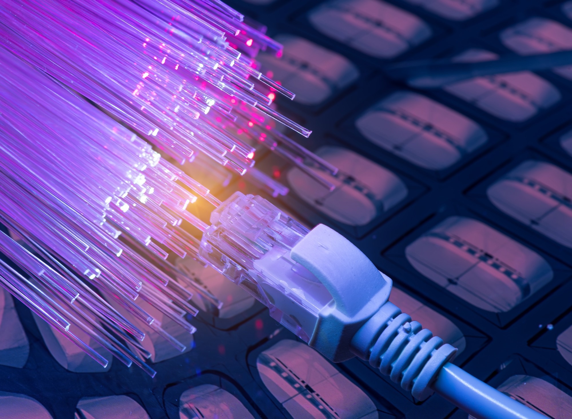
Image Credit: asharkyu/Shutterstock.com
Photonics has emerged as an advanced technology for next-generation computing systems.2 Photonic devices can process data with greater parallelism than electrical devices and can simplify the structure and design of several complex computing systems.1
This article explores recent advances in photonic devices and their applications in computing.
Optical Computing and Photonic Devices
The origin of optical computing dates back to the 1960s when the military utilized coherent optical imaging systems for convolution and correlation tasks.2 Currently, optical computing is generally classified as digital and analog.
Digital optical computing, developed for over 30 years, is based on Boolean logic and uses mechanisms similar to transistor-based computing. However, due to low device integration density, it cannot compete with conventional digital computing.
Alternatively, analog optical computing uses the physical properties of light, such as phase and amplitude, and its interaction with optical devices.1
Photonics involves the production, detection, and manipulation of photons (light) through transmission, emission, signal processing, modulation, switching, amplification, and sensing. Photonic devices like optical fibers and waveguides are widely used in optoelectronic applications.3
The speed of light in photonics devices, including solid-state devices and crystals, is faster than that of electrons in traditional computing chips. Thus, optical systems can compute 1000 times faster than electronic computers, which suffer from limited physical electronic transmission.
Optical fibers can also accommodate more wavelengths than conventional copper wires, providing high transmission bandwidth.3
Advantages of Photonic Devices in Computing
The response time of electrical circuits restricts existing computers. Transmission through a solid medium exhibits limited signal speed and volume and generates heat that damages components. Microscopic electronic equipment also suffers from signal mixing, compromising the system’s reliability.2
In contrast, light does not suffer from time domain restrictions or require insulators. It can simultaneously transmit several photon streams of distinct frequencies without interference and is immune to electromagnetic interference and electrical short circuits.2
Photonic devices are promising for computing applications due to their intrinsic parallelism, low latency, and immunity to environmental noise. They enable instant data processing with minimal energy usage and heat generation.1 Additionally, photonic components are smaller, lighter, and less expensive.2
Optical computing can perform 1 trillion calculations per second, quicker than the best commercial transistors today. It also consumes less energy for state transition due to the single photon-based actuation of optical switches and no cooling requirements.2
Optical materials surpass magnetic materials in storage density and availability. Despite the tiny electronic logic gates used today, interlinking capacitance restricts switching speeds, while optical logic gates exhibit femtosecond switching rates, constrained only by the speed of light.2
Recent Technological Advances
Photonic devices for optical computing, such as logic gates, switches, neural networks, chips, and modulators, are rapidly advancing, overcoming the constraints of existing electrical computers.2 For example, Lightmatter introduced the world’s first Mach-Zehnder interferometer (MZI) integrated chip, "Mars," establishing the viability of large-scale integration of optical-electrical chips.1
A research team at Russia’s Skolkovo Institute of Science and Technology, in collaboration with IBM, developed an extraordinarily energy-efficient optical switch with no cooling requirement, potentially forming the basis for future computers that manage photons instead of electrons. This switch was fabricated using a 35-nm semiconducting organic polymer positioned between highly reflecting surfaces.2
Optalysys, a technology startup, employs innovative optical processing to overcome current computing challenges and expand AI potential for high-resolution image and video applications. Their computing method using photons instead of electrons can accelerate processor-intensive operations while consuming much less energy than silicon processors.2
The rising bandwidth requirements and lower energy consumption have led to optical interconnects replacing electrical interlocks in computing chips. Furthermore, novel phase change materials are being explored for photonic devices such as on-chip modulators and switches as they offer high switching speeds by changing electrical/optical properties.2
Applications in Optical Computing
Photonic devices are being innovatively employed in optical computing to circumvent the difficulties of electronic computing.
For example, photonic chip-based optical neural networks (NNs) are gaining significant attention due to their exceptional adaptability, scalability, and durability. These are used in advanced machine learning and AI techniques for accuracy in tasks like image identification and speech processing. All-optical NNs and optical reservoir computing have been successfully demonstrated by embedding silicon photonic devices.2
A recent study in ACS Photonics explored the application of nanophotonics for neuromorphic optical data storage, inspired by the human brain’s memory capabilities, offering high storage, parallelism, and low power usage. These methods can help develop neuromorphic optical data storage to meet the demands of cloud computing and AI.
Additionally, computing applications involving optical input signals, such as light detection and ranging (LIDAR), image processing, and telecommunications, would greatly benefit from the proposed neuromorphic memories.4
Another recent study, presented at the 22nd Association for Computing Machinery (ACM) Workshop, proposed on-fiber photonic computing for network transponders processing optical data. Augmenting pluggable transponders with such photonic computing systems can provide a backward-compatible method for in-network computing. The proposed on-fiber photonic computing has potential applications in machine learning interpretation, video encrypting, load assessment, and interference recognition.5
Future Outlook
Future ultra-fast computers are expected to employ parallel digital-optical processing, but the practical implications of such hybrid optoelectrical systems need systematic analysis.1,2
The optical-electrical co-package technology should be developed to lower the expense of data transfer between electrical and optical domains. Additionally, current optical transmitters and modulators are designed for communication applications, but optical computing demands a much higher extinction ratio and linearity of photonic devices due to the high bit depth of the input data.1
The existing computing architecture cannot fully benefit from photonic devices due to the high energy requirement for optical-electrical conversion. Current algorithms employ Boolean logic for digital computers, which cannot handle the operators used in optical computing, necessitating the development of specific algorithms for optical computing.1
Continued innovation will help achieve practical and commercially viable photonic solutions for optical computing. Future computers consisting of photons, optical fibers, crystals, thin films, and mirrors instead of electrons and cables might complete a task that a normal computer takes over 10 years to finish in less than an hour.2
More from AZoOptics: Ultrasonic Techniques for Lithium-Ion Battery Diagnostics
References and Further Reading
1. Li, C., Zhang, X., Li, J., Fang, T., Dong, X. (2021). The challenges of modern computing and new opportunities for optics. PhotoniX, 2(1). doi.org/10.1186/s43074-021-00042-0
2. Kazanskiy, NL., Butt, MA., Khonina, SN. (2022). Optical Computing: Status and Perspectives. Nanomaterials. doi.org/10.3390/nano12132171
3. Amiri, I., et al. (2018). Introduction to Photonics: Principles and the Most Recent Applications of Microstructures. Micromachines. doi.org/10.3390/mi9090452
4. Lamon, S., Zhang, Q., Yu, H., Gu, M. (2024). Neuromorphic Optical Data Storage Enabled by Nanophotonics: A Perspective. ACS Photonics. doi.org/10.1021/acsphotonics.3c01253
5. Yang, M., Zhong, Z., Ghobadi, M. (2023). On-Fiber Photonic Computing. Proceedings of the 22nd Association for Computing Machinery (ACM) Workshop on Hot Topics in Networks. doi.org/10.1145/3626111
Disclaimer: The views expressed here are those of the author expressed in their private capacity and do not necessarily represent the views of AZoM.com Limited T/A AZoNetwork the owner and operator of this website. This disclaimer forms part of the Terms and conditions of use of this website.