Apr 22 2010
SII NanoTechnology USA Inc. (SIINT) recently customized designs of their 50mm2 silicon drift detectors (SDD), increasing the detectors’ solid angle, by allowing a close sample-to-detector geometry.
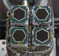 SII NanoTechnology USA designs 4-element silicon drift detector (SDD) arrays.
These improvements increase the high rate capability and permit silicon drift detectors to be placed under a sample at optimal proximity, shortening signal collection time.
“SII NanoTechnology USA has a solid commitment to developing X-ray and XRF solutions that are innovative, clear-cut and cost-saving,” says Gordon Myers, SIINT Vice President of Sales and Marketing. “The new SDDs offer a large solid angle, great energy resolution, and high count rate performance.”
SIINT addressed silicon drift detectors’ large active area by developing a 4-element array with 4-channel electronics. The innovative 4-element SDD spectrometer is being used in high rate synchrotron applications requiring large solid angle and high detection efficiency. “The SDD arrays also replace traditional and bulky liquid nitrogen (LN)-cooled multi-element germanium detectors,” commented Shaul Barkan, Sr., Vice President and Chief Technical Officer.
The 4 silicon drift detector elements are positioned in a square arrangement with heat removed through an innovative heat pipe heat transfer and cools the detectors down using Peltier coolers. The 4-element design has an active area totaling 180mm2 and an output rate of 2Mcps.
SII NanoTechnology USA Inc. also improved a 50mm2 SDD design with a larger solid angle, assembling it into a transmission electron microscope (TEM) at the Electron Microscopy Center at Argonne National Laboratory (ANL). The new design allows the active area of the detector to be placed directly under the sample. This close sample-to-detector geometry, or “close geometry” design, maximizes the solid angle—increasing count rate and improved sensitivity.
“The improved silicon drift detector is ideally suited for the characterization of nanoparticles at high spatial resolution,” says Myers. “Because this characterization has become extremely important in state-of-the-art materials research, SII NanoTechnology USA will continue to develop original nanotechnology equipment for applications such as x-ray spectroscopy and x-ray fluorescence measurements.”