Nov 11 2008
SUSS MicroTec Test Systems (FWB:SMH)(GER:SMH), the premier supplier of wafer-level test solutions for semiconductor devices, today announced the iVista(TM) LC High-Resolution Digital Microscope. Its introduction is timed to meet the increasing need in failure-analysis labs for an advanced microscopy tool capable of delivering high-resolution digital images in conjunction with laser-cutting capabilities.
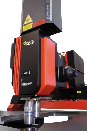 The iVista(TM) LC High-Resolution Digital Microscope was launched today (Photo: Business Wire)
The iVista LC Digital Microscope significantly improves the productivity of operators and engineers by providing a powerful microscopy solution. The unique design of the iVista microscope delivers images with resolution comparable to a 16-megapixel, color CCD. This means that even the tiniest features are quickly and easily identifiable, and unlimited digital zooming provides more detail and not just a pixilated image.
To meet the needs of engineers working in failure-analysis labs, a standard laser port is available to mount laser cutters from all major manufacturers. A high-precision, automated objective changer allows the engineer to switch from a magnification used for navigation to a higher magnification for closer inspection and laser cutting. The iVista LC Microscope also includes an optional polarizer/analyzer unit for liquid-crystal thermography applications and enhanced image contrast. For documentation tasks, the user can save the full-resolution image and the multi-view screen.
Several additional software features in the SPECTRUM™ Vision System are enabled when using the iVista LC Microscope in conjunction with an automated probe system from SUSS MicroTec. Multi-view allows the user to create several freely-defined regions that are magnified and displayed alongside the main view, enabling live observation of specified areas without losing the “big picture”. Multi-cam imaging displays a live image from a separate camera alongside the live image from the iVista LC Microscope. The user can then, for example, monitor contact height with the view from the patented ContactView™ system while observing the position of the wafer and probe tips, eliminating expensive probe-card crashes. Accurate point-to-point measurement and navigation tools using standard objectives are also provided.
“The iVista LC Microscope delivers exactly the tools needed for wafer-level failure analysis.” said Rob Carter, Vice President of Sales and Marketing for SUSS MicroTec Test Systems. “The high-resolution optics along with state-of-the-art digital zooming provide image detail well beyond any similar product. Engineers involved in failure-analysis and design-debug tasks will appreciate the advanced capabilities of the iVista LC, and managers will appreciate the benefits from the productivity gains that can be realized with such a powerful tool.”
The iVista LC Microscope is available for immediate order, and the first units are planned to be shipped in the first quarter of 2009. The system can also be used with a manual probe station or as a stand-alone microscope.