Reviewed by Lexie CornerJun 24 2025
A recent study published in Light: Science & Applications introduced a new method for determining the PN junction depth in a silicon wafer. This technique works at nanometer-scale resolution and is both non-destructive and non-contact.
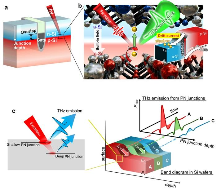
 Concept of the non-contact inspection on the PN junction depth. a, Schematic illustration of the buried channel transistor structure. b, THz emission from the PN junction. Ultrafast photocarrier transport due to the built-in electric field (drift current) generates the THz electromagnetic waves at the PN junction. c, PN junction depth dependence of the THz emission. A, B, and C represent the energy band diagram in Si wafers with different PN junction depths. Photocarrier density at PN junctions depends on their depth. Consequently, the amplitude of the THz emission from the PN junctions is sensitive to the depth. Image Credit: Fumikazu Murakami, Shinji Ueyama et al.
Modern society depends on silicon LSI manufacturing technologies. These technologies aim to increase the density of electronic devices by making components smaller and three-dimensional. However, it has been difficult to quickly and non-destructively evaluate key factors such as internal electric field distribution, carrier transport characteristics, defects, and high-speed response, especially at the wafer scale.
The new method uses a femtosecond laser, also called an ultrashort pulse laser, to illuminate the PN junction within the silicon wafer. The interaction at the PN junction generates photocarriers, enabling the measurement of terahertz electromagnetic waves (THz waves).
When the photo-carriers reach the depletion zone, they accelerate - electrons move toward the n-type Si layer and holes toward the p-type Si layer. The resulting instantaneous current excites THz waves, which then travel to the surface and radiate into space.
The THz waves are essentially generated through the complicated ultrafast photocarrier behavior, but by employing the simple model of the behavior, one can understand the movement of the carriers intuitively and evaluate the depth of the PN junction. Here, we introduce the depth estimation procedure with the simple mode for the THz eave generation from PN junctions for the first time.
Masayoshi Tonouchi, Professor, Research Institute for Interdisciplinary Science, Okayama University
Young scientist Dr. Murakami explained, “It was tricky to use shorter laser wavelengths to excite the shallow PN junctions of Si because the penetration depth of the typical femtosecond laser with a wavelength odd use the f around 800 nm, is much longer than 10 micrometers for Si, and so, we cannot expect that the method is available to characterizing the shallow PN junctions in Si wafers at first. We found that a half wavelength is suitable in the present case, and by tuning the wavelength, one can evaluate shallower junctions more precisely.”
The scientists added, “The complexity of semiconductor devices is accelerating as they aim for higher levels of integration, and the demands and issues for semiconductor wafer and device evaluation technology are increasing. This technology, which enables rapid, non-destructive, and non-contact access to the interior of wafers, which was difficult with existing analysis technology, brings about an important innovation to solve this problem.”
“The results of this research are expected to provide not only the evaluation of wafer structures for devices, but also to provide a comprehensive measurement solution that enables non-contact testing in the semiconductor manufacturing process, which contributes to improving device reliability and reducing the resources consumed in the manufacturing process,” researchers concluded.
Journal Reference:
Murakami, F., et al. (2025) Non-contact and nanometer-scale measurement of PN junction depth buried in Si wafers using terahertz emission spectroscopy. Light: Science & Applications. doi.org/10.1038/s41377-025-01911-0.