Integrated Si photonics adds the core of the two pillar industries of "optoelectronics" and "microelectronics", which is projected to bring new technological revolution in a range of fields such as communication, lighting, detection, display, sensing, imaging, etc. Si lasers are the key to realizing integrated Si photonics.
However, the optical gains of Si are lower than those of III-V compound semiconductors by one order of magnitude or two, because of its indirect bandgap feature. Although the fabrication of matured III-V compound lasers on Si substrates has been suggested to circumvent this issue, the development of all-Si laser is still in great demand for integrated Si photonics, because of its better compatibility with modern Si methods.
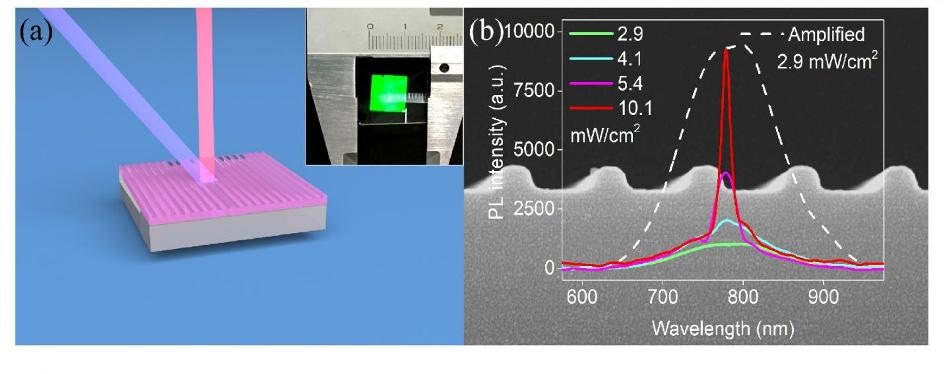 (a) A schematic image of DFB Si laser; Inset: photograph of a fabricated DFB device. (b) Emission spectra of the Si laser as a function of pump power; Background: a cross-sectional SEM image of the DFB structure. (Image credit: ©Science China Press)
Recently, a joint research team headed by Prof. X. Wu, Prof. M. Lu and associate Prof. S.-Y. Zhang from Fudan University built the world's first all-Si laser using Si nanocrystals with high optical gains. First, they improved the Si emission intensity significantly by developing a film growth method for high-density silicon nanocrystals (Physica E, 89, 57-60(2017)). Then, they formulated a high-pressure low-temperature passivation approach, which contributed to a full saturation of dangling bonds, resulting in increased optical gains that were comparable to those attained by indium phosphide (InP) and gallium arsenide (GaAs). On this basis, they engineered and fabricated distributed feedback (DFB) resonance cavities and effectively achieved optically pumped all-Si DFB lasers. The optically pumped all-Si laser also makes the way towards the realization of electrically pumped all-Si laser.
It was discovered that the optical gain of Si nanocrystals was continually enhanced as the passivation took place and finally reached the value comparable to those of InP and GaAs. Lasing features - the polarization dependence, the threshold effect, the significant spectral narrowing and small spread of divergence angle of stimulated emission - were fulfilled, suggesting the realization of an optically pumped all-Si laser. The lasers also displayed reliable repeatability. The lasing peaks of the four extra samples made under the similar fabrication conditions were within the spectral range of 760 nm to 770 nm. The variation in the lasing peak was because of the minor difference in effective refractive indices. The full-width-at-half-maximum (FWHM) of the emission peak was narrowed from ~120 nm to 7 nm when the laser was pumped above threshold. This study is supported by the National Natural Science Foundation of China (51472051, 61275178, 61378080, 61705042) and Shanghai Sailing Program (16YF1400700).