Image Credit: Meiyan Pan, Yifei Fu, Mengjie Zheng, Hao Chen, Yujia Zang, Huigao Duan, Qiang Li, Min Qiu, and Yueqiang Hu
Conventional imaging, on the other hand, depends on the light bending at the surface of the lenses and the progressively accumulating phase change along the propagation.
It is challenging to downscale the size of traditional lenses without the lenses having a sufficient thickness. Due to the restricted performance of a single lens, conventional imaging systems typically include cascade lenses. Consequently, smaller imaging systems present difficulties for traditional optics.
The metalens, a flat lens based on metasurfaces, could provide an alternative to satisfy the increased demand for system integration and device miniaturization. A sudden phase change locally induced by subwavelength features, notably meta-atoms, results in metalens focusing.
For its remarkable efficiencies, all-dielectric metalenses have drawn the most interest. Many degrees of freedom are introduced to manipulate the light wavefront using the planar structure. Then, flat optics that are incredibly thin and light are made possible.
Researchers from Jihua Laboratory and Hunan University in China, along with their colleagues, have highlighted the advancement of dielectric metalenses in compact imaging systems while highlighting the obstacles impeding future advancements in a new review article published in Light: Science & Application to promote the development of metalens-based compact devices.
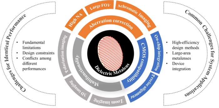
Dielectric metalenses can correct aberrations and engineer dispersion due to their customized wavefront engineering, and they provide a single-piece solution to problems with monochromatic and achromatic focusing.
Due to the high degree of freedom in regulating light, numerous functionalities can even be accommodated within the same common aperture of a single metalens.
Single-piece metalenses have a number of chances to replace their complex conventional equivalents, as seen by recent advancements in diverse metalens-based applications such as three-dimensional imaging, real-time polarization imaging, and optical analog computing.
Despite the enormous progress made thus far, it is noted that several obstacles still need to be overcome before metalens-based imaging systems can be developed practically.
The researchers stated, “High focusing efficiency is challenging for high-NA metalenses due to the fundamental phase discretization and diffraction constraints. The breakthrough broadband achromatic feature of metalens suffers from some fundamental constraints, design limitations, and fabrication challenges. Moreover, conflicts in metalens parameters and aberration correction capabilities should be manipulated.”
“Regarding multifunctional metalenses, the overall efficiency is limited by not only the efficient component of power but also the crosstalk among the sub-units. Balancing the performances among different focal spots is also a tough task.”
“In addition, common challenges are hindering further development of dielectric metalens-integrated systems, including limitations of conventional design methods, the scaling up of dielectric metalenses, and the approaches for integrated devices,” added researchers.
They further stated, “In turn, these challenges provide some possible future development directions of metalenses: (i) New strategies to break the conflicts among metalens performances. (ii) Multifunctional and reconfigurable metalenses that could replace complicated configurations of conventional optics. (iii) High-efficiency design methods for high-performance metalenses. (iv) High-efficiency fabrication and mass manufacturing methodologies for large-area metalenses.”
The researchers concluded, “By addressing the present challenges of metalenses and combining the non-local optics, we envision that metalens-based imaging systems would be increasingly compact and widely employed in future applications, ranging from camera modules for consumer photography and autonomous vehicles to wearable displays for AR/VR/MR and machine vision, to bioimaging and endoscopy, to signal processing and optical computation.”
Journal Reference:
Pan, M., et al. (2022) Dielectric metalens for miniaturized imaging systems: progress and challenges. Light: Science & Applications. doi:10.1038/s41377-022-00885-7.