Semiconductor devices are integral to modern electronics, enabling everything from computers and smartphones to advanced sensors and power systems. As these devices continue to scale down in size while increasing in complexity, ensuring their performance and reliability presents significant challenges for manufacturers. Advanced optical techniques have become indispensable across semiconductor development and manufacturing, offering the precision and sensitivity required for cutting-edge technology. This article explores how key optical methodologies are applied to inspection, metrology, and analysis at various stages of semiconductor research, development, and volume manufacturing.
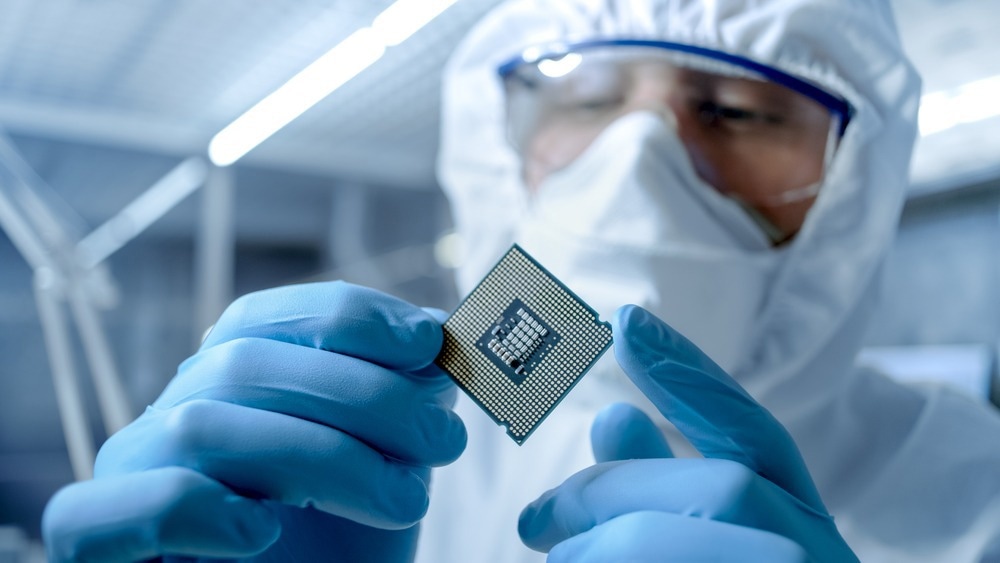
Image Credit: Gorodenkoff/Shutterstock.com
Optical testing capitalizes on the fundamental principle that the interaction between light and material can alter its polarization characteristics, contingent upon optical properties such as film thickness, refractive index, and surface texture.
These techniques offer the distinct advantage of real-time monitoring during manufacturing, ensuring high yields and cost efficiency. In addition, their non-destructive nature ensures that semiconductor devices remain intact and unaltered during measurement. These attributes are vital for quality control and reliability assessment, as they allow for thorough evaluations without compromising the devices' integrity.
Moreover, optical testing expedites the product development cycle, fostering innovation across various stages of semiconductor device development.
In-Line Metrology with Ellipsometry
Maintaining strict process control is crucial for achieving yields with nanoscale semiconductor manufacturing. Optical techniques such as ellipsometry provide high-precision metrology of critical dimensions and film properties, enabling real-time process monitoring and excursion detection.
Ellipsometry determines film thickness and optical constants with angstrom resolution by measuring polarized reflectance. This precision is crucial for optimizing semiconductor components like LEDs, lasers, photodetectors, HFETs, and HEMTs.
Spectroscopic ellipsometry is instrumental in metrology tasks involving intricate layer stacks, including high-K dielectrics and finFET structures. It finds utility in monitoring numerous semiconductor processes, ranging from chemical vapor deposition (CVD) and atomic layer deposition (ALD) to epitaxy, thermal oxidation, and chemical mechanical polishing (CMP). Additionally, it provides valuable insights into parameters like refractive index, extinction coefficient, and dielectric function.
Liquid crystal modulation spectroscopic ellipsometry is a powerful tool for characterizing compound semiconductor heterostructures like AlGaN/GaN. Its MM-16 spectroscopic ellipsometer simplifies the determination of film thickness and optical properties, even for thick films. This is vital for designing optoelectronic devices and creating calibration curves to determine alloy composition efficiently, especially the aluminum content.
Furthermore, this non-destructive technique can be used on SiGe, II-VI, and classical III-V semiconductors, offering valuable insights into layer structures, interfaces, roughness, anisotropy, and optical constants (n,k). These insights are critical for understanding material characteristics like band gaps and absorption coefficients.
Semiconductor Quality Control Using Raman Spectroscopy
Raman spectroscopy analyzes the inelastically scattered light from a material to provide chemical and structural information in a non-destructive manner. It can identify contaminants, measure crystal quality, and detect strain in silicon structures for semiconductor applications.
Raman's microspectroscopy variant plays a crucial role in pinpointing contaminants once they have been located. Its effectiveness lies in its ability to analyze small samples and its vibrational technique, which can identify various organic components.
Furthermore, Raman spectroscopy is instrumental in assessing the crystal structure of silicon. It can distinguish between different silicon crystal forms, such as polycrystalline and amorphous structures. This capability is valuable in semiconductor manufacturing processes.
Another critical application of Raman spectroscopy is detecting strain in silicon structures. It achieves this by measuring lattice vibrations, which are sensitive to strain. This feature makes Raman spectroscopy an ideal tool for applications like monitoring wafers and ensuring the structural integrity of semiconductor devices.
Operational Environment Analysis with Dual-Beam Interferometry
Dual-beam interferometry uses two laser beams configured in a Michelson interferometer setup to simultaneously probe the refractive index changes at different spots on a semiconductor device. This provides absolute phase shift measurements at two locations on the device with sub-nanosecond time resolution. It enables the investigation of ultrafast carrier dynamics and device behavior under electrical stress conditions by resolving the temporal response at different locations.
Dual-beam interferometry is thus a unique tool for characterizing semiconductor devices under operational environments with high spatial and temporal resolution.
Photoluminescence for Compound Semiconductor Characterization
Photoluminescence is widely used to characterize optoelectronic materials like III-V compound semiconductors. It employs lasers to generate carriers within semiconductor materials, where carrier recombination yields photons that unveil crucial insights into a material's electronic properties.
This technique serves diverse purposes in semiconductor testing. Firstly, it accurately determines the bandgap of new compound semiconductors, a pivotal factor in understanding their characteristics. Additionally, it excels at detecting impurity levels and specific defects, leveraging the analysis of energy levels and photoluminescence intensity. Furthermore, it assesses material quality and recombination mechanisms, particularly important in devices like lasers, detectors, LEDs, and high-speed components, revealing insights into crystal imperfections.
Photoluminescence also shines in evaluating epitaxial layer quality. Its intensity inversely correlates with defect density, making it a valuable indicator of the quality of these layers. Moreover, it provides essential information regarding wavelength and uniformity across wafers, facilitating the prediction of device performance. Lastly, photoluminescence's ability to measure emission spectra enables it to determine the composition of quaternary materials and identify variations due to temperature changes, a crucial aspect of epitaxial growth control.
Navigating the Nano-Era with Light
The industry's relentless pace of miniaturization into the nano dimensions places enormous demands on process control, inspection, metrology, and analysis. Due to their high resolution, sensitivity, and non-destructive characteristics, optical techniques have become indispensable tools for continuing Moore's Law. As a result, developing novel optical approaches and enhancing existing capabilities will remain vital for semiconductor manufacturing to keep pace with escalating technological and economic challenges.
More from AZoOptics: How is Raman Spectroscopy Used to Study Crystallography?
References and Further Reading
CRAIC Technologies. (2023). UV-visible-NIR, Fluorescence, Photoluminescence & Raman Microspectrophotometers. [Online]. Available at: https://www.microspectra.com/29-support/solutions-1/294-raman-for-semiconductor
Horiba. (2023). Spectroscopic Ellipsometry of Compound Semiconductors: AlxGa1-xN / GaN Heterostructures. [Online]. Available at: https://www.horiba.com/int/scientific/applications/semiconductors/pages/spectroscopic-ellipsometry-of-compound-semiconductors-alxga1-xn-gan-hetero-structures/
Horiba. (2023). Optical Characterization of Organic Semiconductors by Spectroscopic Ellipsometry. [Online]. Available at: https://www.horiba.com/int/scientific/applications/semiconductors/pages/optical-characterization-of-organic-semiconductors-by-spectroscopic-ellipsometry/
Dubec, V. (2005). Advanced optical interferometric methods for nanosecond mapping of semiconductor devices under high energy pulses (Doctoral dissertation). Available at: https://repositum.tuwien.at/handle/20.500.12708/12797
Reader, A., Moore, C., Brinker, R., & Hennessy, J. (2001). Optical testing techniques for new semiconductor processes and new materials. Surface and Interface Analysis: An International Journal devoted to the development and application of techniques for the analysis of surfaces, interfaces and thin films, 31(10), 1000-1011. https://doi.org/10.1002/sia.1135
Disclaimer: The views expressed here are those of the author expressed in their private capacity and do not necessarily represent the views of AZoM.com Limited T/A AZoNetwork the owner and operator of this website. This disclaimer forms part of the Terms and conditions of use of this website.