Demonstrating a super-steep-slope transistor facilitated by exotic optical and electronic properties has triggered a widespread search for van der Waals (vdW) combination and stacking order with unusual band structure and the appropriate size optoelectronic ability for maintaining practical requirements of advanced optical communications and sensing technologies. This article looks at a recent study titled, 'Hybrid Dirac semimetal-based photodetector with efficient low-energy photon harvesting' published in Light: Science & Applications.
Photovoltaic systems based on vdW heterostructures with unique band-alignment features, in particular, have revolutionized early photonic technology in the visible or near-infrared ranges.
However, the main photodetection technological bottlenecks are in the low-photon-energy range of the electromagnetic spectrum because the detectable wavelength is exacerbated by selective bandgap dependence and the complexity of efficiently converting photon energy into electrical signal within a small nanoscale active area.
Platinum diselenide (PtSe2), a broad family of transition metal dichalcogenides, has the distinct advantage of broadband light absorption due to type-II Dirac fermions. PtSe2 and similar Van der Waals phototransistors have demonstrated high-efficiency photoelectric conversion in the visible and infrared regions.
As a result, PtSe2 is a good option for developing novel optoelectronic devices that use the topology of its energy bands and the Berry-curvature-induced phenomena.
With its diverse symmetry-breaking activity, the PtSe2 topological Dirac semimetal offers unparalleled chances to research Dirac fermiology beyond the early milestones of graphene-based optoelectronics in this burgeoning discipline.
Understanding the dominant role of nonequilibrium states, particularly in the low-energy THz band, is extremely important in device applications, as it is necessary to perform effective charge separation and handle technology-related difficulties.
The unique photoconductive behavior of PtSe2 and its van der Waals integration provide a flexible platform for the synergistic manipulation of optoelectronic characteristics for high-performance THz detection via geometrical as well as band-structure engineering in this research.
In the skin-depth regime, researchers implement optically excited hot electrons under ultra-strong interaction with near-field, followed by quasi-equilibrium transport obliterating the power-hungry drawbacks, with the decrease of thermal-agitation noise and the accomplishment of chip-level integration for low-energy photodetection.
Methodology
The CuSe flux method was utilized to generate single crystals of PtSe2 for this study. In an alumina crucible with an alumina frit, mixtures of Pt (99.99%) foil, Cu (99.99%) foil, and Se ingot (99.999%) were mixed in the ratio of 1:6:8 and sealed in an evacuated quartz tube. The Laue diffraction pattern of PtSe2 along the [0 0 1] direction is shown in the inset, demonstrating excellent crystallization of the crystal based on the crisp spots in the Laue pattern.
After removing a Shirley-type backdrop, Pt-4f core levels were decomposed using Doniach-Šunjić doublet line shapes, while Se-3d core levels were decomposed using Voigt line shape functions.
The near-field experiment was carried out with a near SNOM system based on reflecting optics, which allowed the system to be used throughout a wide wavelength range, from visible to THz. The neaSNOM integrated THz-TDS is based on a THz emitter/receiver combination with an fs laser-driven semiconductor antenna.
Semiconductor Parameter Analyzer (B2912A) was used to measure the electrical characteristics of the devices in variable voltage mode. Data was collected using a custom-built optical setup for photoresponse measurements.
Results
A bow-tie antenna with a sub-wavelength gap is modeled using the finite difference time domain method (FDTD), with the photoactive area varying from 30 to 100 nm in the metallic nanoslit, to demonstrate the capacity of optical-field augmentation (Figures 1b, c).
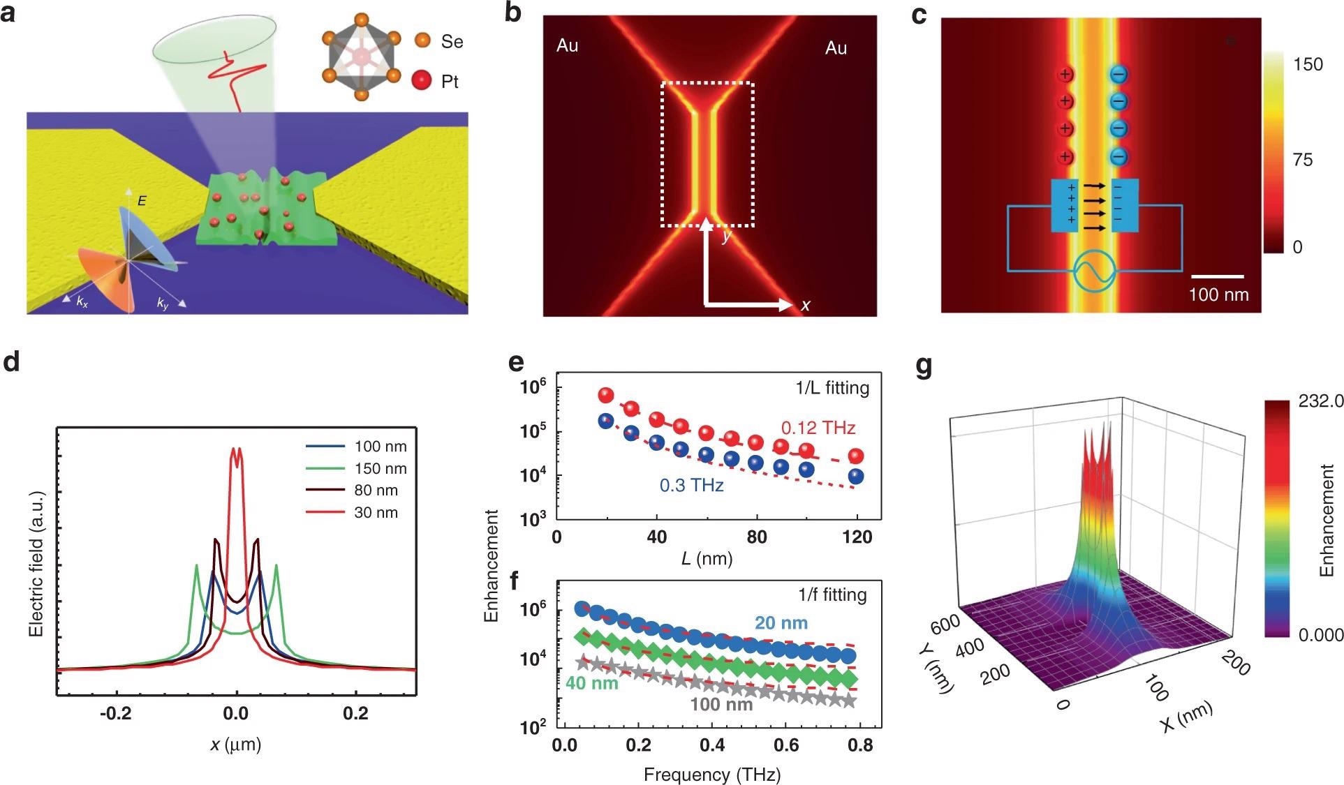
Figure 1. Scaling law of plasmonic near-field characteristic toward the skin-depth regime. (a) Schematics of the bow-tie antenna-assisted device. (b, c) The cross-section view of the simulated electric field intensity normalized to incident one marks the power-gain around the nanochannel at 0.3 THz electromagnetic waves. Localized oscillating electric field enhancement in the sub-100 nm channel by light-induced current charges. (d) The profile of electric field distribution along the x-axis. (e, f) The scaling of electric field enhancement derived from FDTD method versus channel length and incident frequency. (g) The spatial distribution of the electric field near the 100 nm gapped channel substantiates the strong focusing induced by the oscillating charge. Image Credit: Wang, et al., 2022
The figure of an effective line-capacitor operated by light-induced alternating currents, as shown in Figures 1d, e, shows that the electric field intensity will continue to develop even when the gap size reduces and approaches the skin-depth limit. Figure 1f demonstrates how lowering gap-slit widths approach the skin-depth limit successfully focuses THz waves in the λ/30000 metal slit, resulting in continuous optical-field augmentation.
The channel areas are self-aligned by EBL and then evaporated with Ti/Au again at a varied tilt angle (30° < θ <70 °) in Figure 2a, b, to maintain the in-plane asymmetry for the unilateral movement of the nonequilibrium carriers.
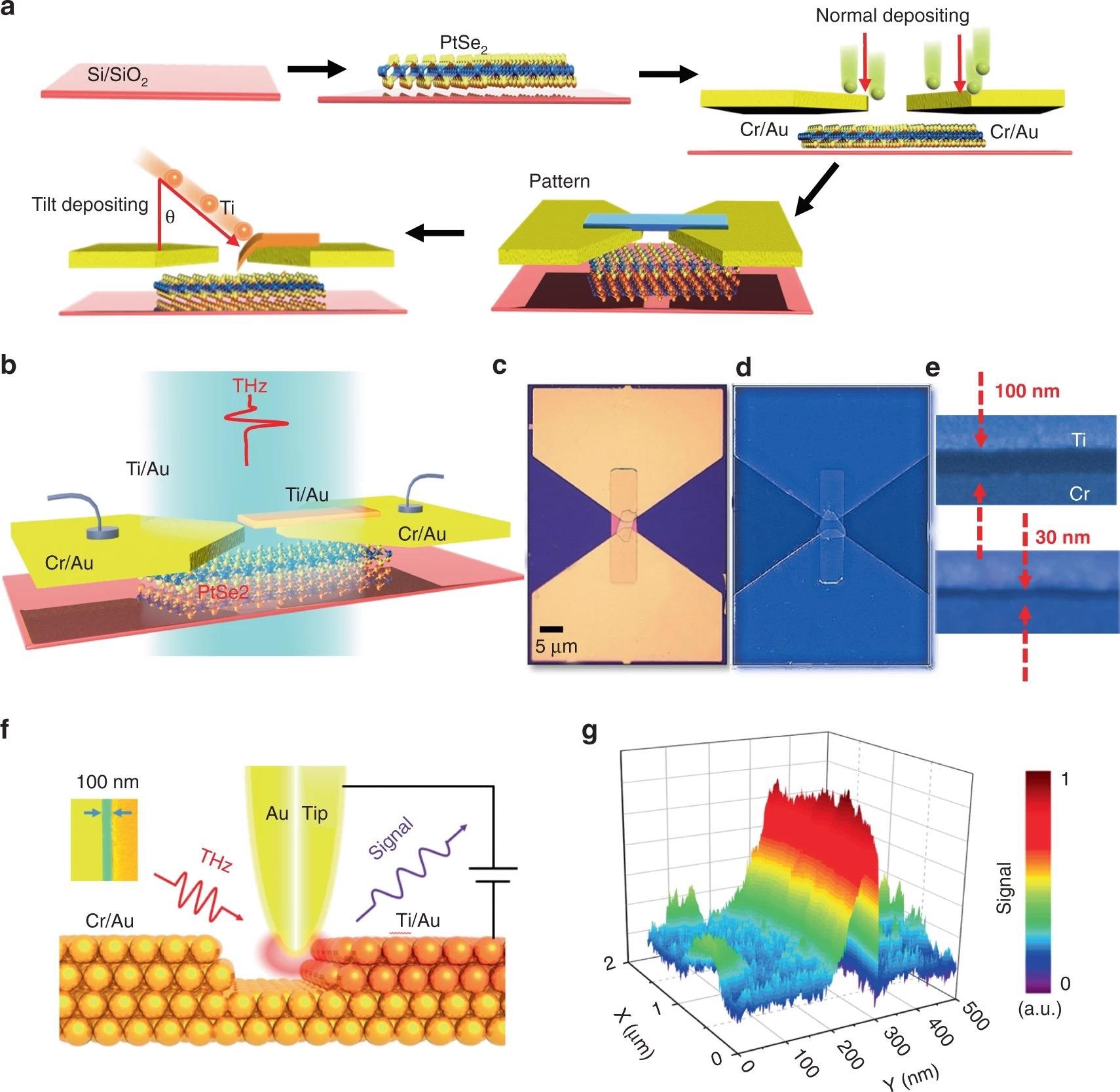
Figure 2. The nanogap slit fabrication technology and s-SNOM. (a) The nanogap slit device fabrication process, including PtSe2 fabrication, ultraviolet lithography, lift-off processes, and tilt deposition. (b) Schematic of the bow-tie antenna-assisted device. (c–e) Optical microscopy and false-color SEM images of the PtSe2 nanogap slit device with a typical channel length (100 nm and 30 nm). (f) The near-field images are taken around the slit area using broadband illumination. (g) Stereograph of the near-field signal. Image Credit: Wang, et al., 2022
Two polymethyl pentene (TPX) lenses collimate and focus the incoming THz beam into a circular spot with the spatial intensity profile shown in Figure 3a.
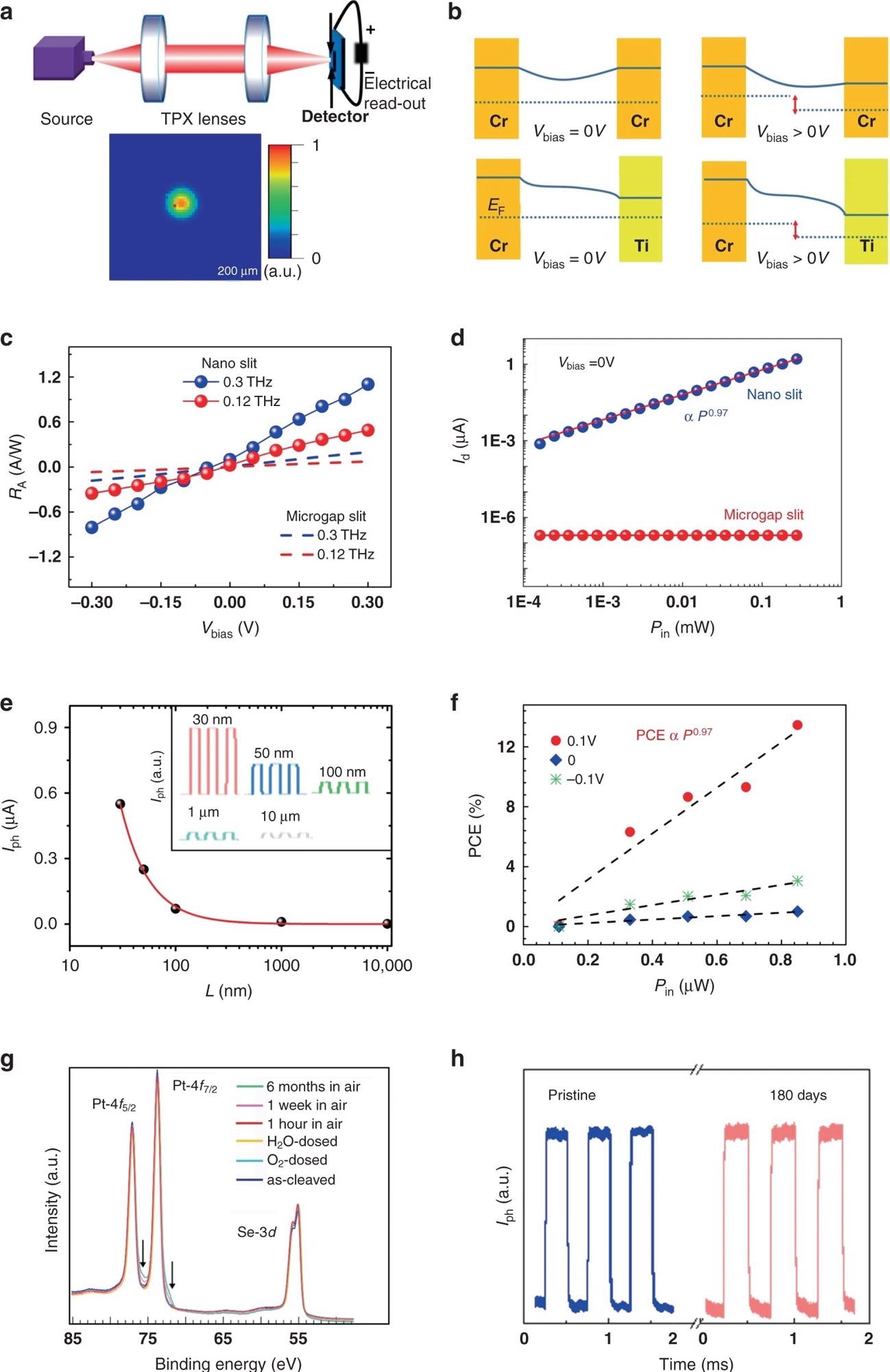
Figure 3. Characteristics of the PtSe2 low-energy photon detector. (a) Schematic diagram of the experimental geometry, with photon-beam spot profile (diameter: 800 μm), derived from two-dimensional scanning of the photodetector. (b) The band diagram at the different metal junction regions with/without bias. (c) Bias dependence of responsivity at 0.12 THz and 0.3 THz for different channel lengths. (d) The measured photocurrent vs. output power Pin, with the power, varied from 0.3 μW to 300 μW. The channel length of the typical microgap slit and nanoslit device is 4 μm and 100 nm, respectively. (e, f) The conversion efficiency of the nanogap slit photodetector versus the incident power at room temperature. (g) Pt-4f and Se-3d core levels, measured at a photon energy of 400 eV. (h) Time-resolved photo signal of PtSe2-based nanogap slit photodetector at Vbias = 0 V. Image Credit: Wang, et al., 2022
When PtSe2 is combined with graphene, it can provide integrated behavior with unique structural characteristics and properties that the separate components lack and increased functional performance above graphene or PtSe2 alone (Figure 4a).
Imaging technologies in non-invasive inspection procedures are critical for maximizing the vast potential of low-energy photon processing. As a result, researchers undertake low-energy photon imaging of samples hidden behind opaque materials, such as single-view scans of a young leaf, to assess the technical potential of the PtSe2-based detector (Figure 4g).
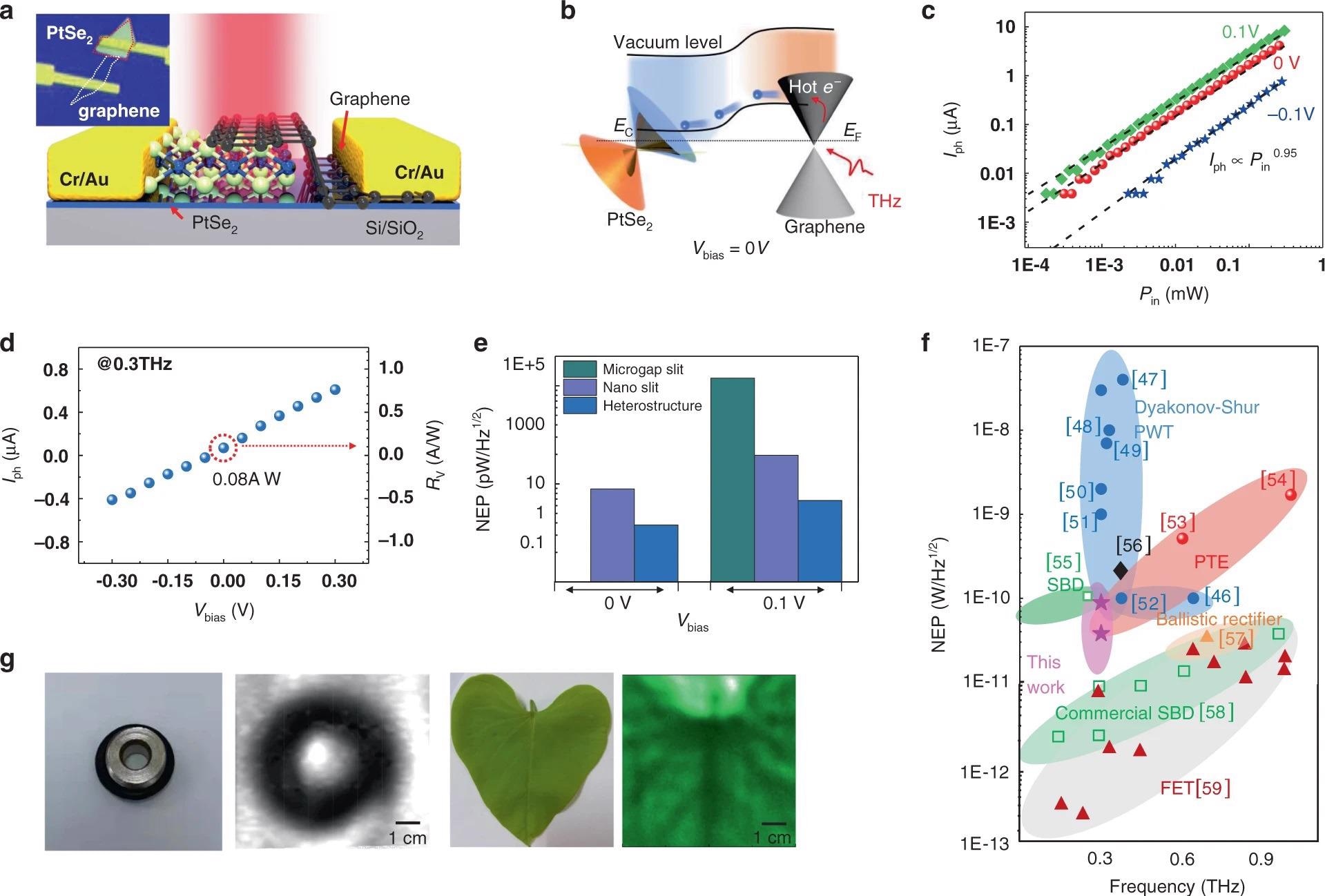
Figure 4. Characteristics of the PtSe2/graphene low-energy photon detector. (a) Schematic diagram of the device architecture. Inset: the optical micrograph of the device. (b) Schematic band diagram of PtSe2-graphene heterostructure. (c) The measured photocurrent vs. incident power Pin with the power varied from 0.3 μW to 300 μW. (d) Bias dependence of photocurrent at 0.3 THz, yielding responsivity of 0.08 A/W at unbiased voltage. (e) Comparisons of NEP at 0.3 THz among pristine metal-PtSe2-metal, asymmetric nanogap slit device, and PtSe2-graphene vdW heterostructure. (f) Summary of the measurement of our devices and comparison with past works. PTE = photo-thermoelectric effect, Dyakonov-Shur PWT = Dyakonov-Shur plasma wave theory, SBD = Schottky barrier diode, FET = Field-Effect Transistors. Black phosphorus (BP)/hBN heterostructure, BP FET, Bi2Te(3−x)Sex FET, BP nano-transistors, Nanowire (NW) Field-Effect Transistors, Se-doping InAs NWs FETs, Hg1–xCdxTe, CVD Graphene, Antenna Enhanced Graphene, InGaAs Schottky barrier diode (SBD) array, Graphene ballistic rectifier, Commercial Golay, Commercial VDI, SBD FETs. The pick represents the performance of nanoslit and heterostructure devices, respectively. (g) The optical picture of a fresh leaf and a metallic ring used in the imaging and 0.3 THz transmissions nondestructive image of the fresh leaf demonstrates the leaf vein, which partly contains more moisture. Image Credit: Wang, et al., 2022
Noise-equivalent power (NEP) is another important figure of merit for evaluating a photodetector’s performance in practical applications. The PtSe2-based detector offers the potential for real-time THz imaging when compared with the other thermal detectors. Another benefit of PtSe2-based detectors for THz imaging applications is the ability to build micro gap detectors in arrays.
Discussion
Researchers have shown a new multilayer PtSe2-based low-energy photon detector with a bow-tie antenna that precisely channels the incident THz electromagnetic wave onto the detector’s tiny photoactive area. With an ultimate optical responsivity of 0.2 A/W (0 V, 0.3 THz) and a NEP of 38 pW/Hz0.5, the low-energy photon detectors allow room-temperature rectification of a low-energy photon signal.
Surprisingly, the observed sensitivity performances are being used in a practical situation for non-destructive imaging of macroscopic objects.
Scientists have also developed techniques to increase device performance by optimizing (i) the antenna, (ii) Ohmic contacts, (iii) van der Waals heterojunctions, and (iv) absorption using precisely engineered subwavelength structures. Nonetheless, further improvements in the sensitivity of PtSe2-based low-energy photon detectors may be possible.
Conclusion
Researchers have confirmed the chemical inertness of PtSe2 surfaces to ambient gases (oxygen and water) and, as a result, the long-term durability of PtSe2-based devices using synchrotron-based surface-science methods.
This work opens new possibilities for the simple realization of portable room-temperature, low-photon detectors with high sensitivity, fast operation, and low NEP, with significant advantages over current technologies, due to the superior ambient stability and excellent potential for scalable synthesis of PtSe2.
These findings mark a significant step forward in creating high-performance photonic devices such as low-energy photon cameras, photodetectors, modulators, and other devices.
Journal Reference:
Wang, L., Han, L., Guo, W., Zhang, L., Yao, C., Chen, Z., Chen, Y., Guo, C., Zhang, K., Kuo, C.N. and Lue, C.S. (2022) Hybrid Dirac semimetal-based photodetector with efficient low-energy photon harvesting. Light: Science & Applications, 11(1), pp.1-10. Available Online: https://www.nature.com/articles/s41377-022-00741-8.
References and Further Reading
- Britnell, L., et al. (2012) Field-effect tunneling transistor based on vertical graphene heterostructures. Science, 335, pp. 947–950. doi.org/10.1126/science.1218461.
- Liu, Y., et al. (2021) Promises and prospects of two-dimensional transistors. Nature, 591, pp. 43–53. doi.org/10.1038/s41586-021-03339-z.
- Akinwande, D.,et al. (2014). Two-dimensional flexible nanoelectronics. Nature Communications, 5, p. 5678. doi.org/10.1038/ncomms6678.
- Bahramy, M. S. et al. (2018) Ubiquitous formation of bulk Dirac cones and topological surface states from a single orbital manifold in transition-metal dichalcogenides. Nature Materials. 17, pp. 21–28. doi.org/10.1038/nmat5031.
- Noh, H. J. et al. (2017) Experimental realization of type-II Dirac fermions in a PdTe2 superconductor. Physical Review Letters, 119, p. 016401. doi.org/10.1103/PhysRevLett.119.016401.
- Yan, M. Z., et al. (2017) Lorentz-violating type-II Dirac fermions in transition metal dichalcogenide PtTe2. Nature Communications. 8, p. 257. doi.org/10.1038/s41467-017-00280-6.
- Clark, O. J., et al. (2018) Fermiology and superconductivity of topological surface states in PdTe2. Physical Review Letters, 120, p. 156401. doi.org/10.1103/PhysRevLett.120.156401.
- Wu, F., et al. (2019) High efficiency and fast van der Waals hetero-photodiodes with a unilateral depletion region. Nature Communications, 10, p. 4663. doi.org/10.1038/s41467-019-12707-3.
- Akamatsu, T., et al. (2021) A van der Waals interface that creates in-plane polarization and a spontaneous photovoltaic effect. Science, 372, pp. 68–72. doi.org/10.1126/science.aaz9146.
- Li, Y. W., et al. (2017) Topological origin of the type-II Dirac fermions in PtSe2. Physical Review Materials, 1, p. 074202. doi.org/10.1103/PhysRevMaterials.1.074202.
- Li, Z. G., et al. (2018) Observation of negative longitudinal magnetoresistance in the type-II Dirac semimetal PtSe2. Physical Review B, 98, p. 165441. doi.org/10.1103/PhysRevB.98.165441.
- Zeng, L. H., et al. (2018) Ultrafast and sensitive photodetector based on a PtSe2/silicon nanowire array heterojunction with a multiband spectral response from 200 to 1550 nm. NPG Asia Materials, 10, pp. 352–362. doi.org/10.1038/s41427-018-0035-4.
- Wang, G. Z., et al. (2021) Layered PtSe2 for sensing, photonic, and (Opto-)electronic applications. Advance Materials. 33, p. 2004070. doi.org/10.1002/adma.202004070.
- Wu, D., et al. (2018) Design of 2D layered PtSe2 heterojunction for the high-performance, room-temperature, broadband, infrared photodetector. ACS Photonics, 5, pp. 3820–3827. doi.org/10.1021/acsphotonics.8b00853.
- Ji, Z. R., et al. (2019) Spatially dispersive circular photogalvanic effect in a Weyl semimetal. Nature Materials. 18, pp. 955–962. doi.org/10.1038/s41563-019-0421-5.
- Xu, S. Y., et al. (2018) Electrically switchable Berry curvature dipole in the monolayer topological insulator WTe2. Nature Physical, 14, pp. 900–906. doi.org/10.1038/s41567-018-0189-6.
- Liu, J., et al. (2020) Semimetals for high-performance photodetection. Nature Materials, 19, pp. 830–837. doi.org/10.1038/s41563-020-0715-7.
- Morimoto, T & Nagaosa, N (2016) Topological nature of nonlinear optical effects in solids. Science Advances, 2, p. e1501524. doi.org/10.1126/sciadv.1501524.
- Ma, Q., et al. (2017) Direct optical detection of Weyl fermion chirality in a topological semimetal. Nature Physical, 13, pp. 842–847. doi.org/10.1038/nphys4146.
- Basko, D (2011) A photothermoelectric effect in graphene. Science, 334, pp. 610–611. doi.org/10.1126/science.1214560.
- Lara-Avila, S., et al. (2019) Towards quantum-limited coherent detection of terahertz waves in charge-neutral graphene. Nature Astronomy, 3, pp. 983–988. doi.org/10.1038/s41550-019-0843-7.
- Viti, L., et al. (2020) HBN-encapsulated, graphene-based, room-temperature terahertz receivers, with high speed and low noise. Nano Letters, 20, pp. 3169–3177. doi.org/10.1021/acs.nanolett.9b05207.
- Zhao, Y. D., et al. (2017)High-electron-mobility and air-stable 2D layered PtSe2 FETs. Advanced Materials, 29, p. 1604230. doi.org/10.1002/adma.201604230.
- Zhang, K. N., et al. (2017) Experimental evidence for type-II Dirac semimetal in PtSe2. Physical Review B, 96, p. 125102. doi.org/10.1103/PhysRevB.96.125102.
- Li, Z. Q., et al. (2019) 8.8 GHz Q-switched mode-locked waveguide lasers modulated by PtSe2 saturable absorber. Optics Express, 27, pp. 8727–8737. doi.org/10.1364/OE.27.008727.
- Yan, M. Z., et al. (2017) High quality atomically thin PtSe2 films grown by molecular beam epitaxy. 2D Materiasl, 4, p. 045015.
- Sadhukhan, K., et al. (2020) Novel undamped gapless plasmon mode in a tilted type-II Dirac semimetal. Physical Review Letters, 124, p. 046803. doi.org/10.1103/PhysRevLett.124.046803.
- Zhang, W. X., et al. (2014) Two-dimensional semiconductors with possible high room temperature mobility. Nano Research, 7, pp. 1731–1737. doi.org/10.1007/s12274-014-0532-x.
- Seo, M. A., et al. (2009) Terahertz field enhancement by a metallic nano slit operating beyond the skin-depth limit. Nature Photonics, 3, pp. 152–156. doi.org/10.1038/nphoton.2009.22.
- Jiang, W., et al. (2019) Large-area high quality PtSe2 thin film with versatile polarity. InfoMat, 1, pp. 260–267. doi.org/10.1002/inf2.12013.
- Matsuda, T., et al. (2020) Room-temperature terahertz anomalous Hall effect in Weyl antiferromagnet Mn3Sn thin films. Nature Communications, 11, p. 909. doi.org/10.1038/s41467-020-14690-6.
- Vicarelli, L., et al. (2012) Graphene field-effect transistors as room-temperature terahertz detectors. Nature Materials, 11, pp. 865–871. doi.org/10.1038/nmat3417.
- Tong, J. C., et al. (2017) Surface plasmon induced direct detection of long wavelength photons. Nature Communications, 8, p. 1660. doi.org/10.1038/s41467-017-01828-2.
- Castilla, S., et al. (2019) Fast and sensitive terahertz detection using an antenna-integrated graphene pn junction. Nano Letters, 19, pp. 2765–2773. doi.org/10.1021/acs.nanolett.8b04171.
- Koppens, F. H. L., et al. (2014) Photodetectors based on graphene, other two-dimensional materials and hybrid systems. Nature Nanotechnology, 9, pp. 780–793. doi.org/10.1038/nnano.2014.215.
- Rogalski, A., et al. (2019) Two-dimensional infrared and terahertz detectors: outlook and status. Applied Physics Reviews, 6, p. 021316. doi.org/10.1063/1.5088578.
- Qiu, Q X & Huang, Z M (2021) Photodetectors of 2D materials from ultraviolet to terahertz waves. Advance Materials, 33, p. 2008126. doi.org/10.1002/adma.202008126.
- Safaei, A., et al. (2019) Dirac plasmon-assisted asymmetric hot carrier generation for room-temperature infrared detection. Nature Communications, 10, p. 3498. doi.org/10.1038/s41467-019-11458-5.
- Cai, X. H., et al. (2014) Sensitive room-temperature terahertz detection via the photothermoelectric effect in graphene. Nature Nanotechnology, 9, pp. 814–819. doi.org/10.1038/nnano.2014.182.
- Wu, T. H., et al. (2019) Efficient and stable CsPbI3 solar cells via regulating lattice distortion with surface organic terminal groups. Advance Materials, 31, p. 1900605. doi.org/10.1002/adma.201900605.
- Li, Z. T., et al. (2013) Effect of airborne contaminants on the wettability of supported graphene and graphite. Nature Materials, 12, pp. 925–931. doi.org/10.1038/nmat3709.
- Island, J. O., et al. (2015) Environmental instability of few-layer black phosphorus. 2D Materials, 2, p. 011002. doi.org/10.1088/2053-1583/2/1/011002
- Morishita, T & Spencer, M J S (2015) How silicene on Ag (111) oxidizes: microscopic mechanism of the reaction of O2 with silicene. Scientific Reports, 5, p. 17570. doi.org/10.1038/srep17570.
- Balandin, A A (2013) Low-frequency 1/f noise in graphene devices. Nature Nanotechnology, 8, pp. 549–555. doi.org/10.1038/nnano.2013.144.
- Viti, L., et al. (2016) Heterostructured hBN-BP-hBN nanodetectors at terahertz frequencies. Advance Materials, 28, pp. 7390–7396. doi.org/10.1002/adma.201601736.
- VDI (2020) Available at: https://www.vadiodes.com/en/.
- Viti, L., et al. (2015) Black phosphorus terahertz photodetectors. Advance Materials, 27, pp. 5567–5572. doi.org/10.1002/adma.201502052.
- Viti, L., et al. (2016) Plasma-wave terahertz detection mediated by topological insulators surface states. Nano Letters, 16, pp. 80–87. doi.org/10.1021/acs.nanolett.5b02901.
- Viti, L., et al. (2016) Efficient Terahertz detection in black-phosphorus nano-transistors with selective and controllable plasma-wave, bolometric and thermoelectric response. Scientific Reports, 6, p. 20474. doi.org/10.1038/srep20474.
- Vitiello, M. S., et al. (2012) Room-temperature terahertz detectors based on semiconductor nanowire field-effect transistors. Nano Letters, 12, pp. 96–101. doi.org/10.1021/nl2030486.
- Romeo, L., et al. (2013) Nanowire-based field effect transistors for terahertz detection and imaging systems. Nanotechnology, 24, p. 214005. doi.org/10.1088/0957-4484/24/21/214005.
- Zabudsky, V., et al. (2010) Detection of terahertz and sub-terahertz wave radiation based on hot-carrier effect in narrow-gap Hg1–xCdxTe. Opto-Electronics Review, 18, pp. 300–304. doi.org/10.2478/s11772-010-1026-7.
- Zak, A., et al. (2014) Antenna-integrated 0.6 THz FET direct detectors based on CVD graphene. Nano Letters, 14, pp. 5834–5838. doi.org/10.1021/nl5027309.
- Tong, J. Y., et al. (2015) Antenna enhanced graphene THz emitter and detector. Nano Letters, 15, pp. 5295–5301. doi.org/10.1021/acs.nanolett.5b01635.
- Han, S. P., et al. (2013) InGaAs Schottky barrier diode array detector for a real-time compact terahertz line scanner. Optics Express, 21, pp. 25874–25882. doi.org/10.1364/OE.21.025874.
- TYDEX, Golay (2020) Available at: http://www.tydexoptics.com/products/thz_devices/golay_cell/.
- Auton, G., et al. (2017) Terahertz detection and imaging using graphene ballistic rectifiers. Nano Letters, 17, pp. 7015–7020. doi.org/10.3390/s21092909.
- Javadi, E., et al. (2021) Sensitivity of field-effect transistor-based terahertz detectors. Sensors, 21, p. 2909. doi.org/10.3390/s21092909.