A scanning electron microscope (SEM) scans a material with a focused beam of electrons to create images. When electrons collide with atoms in a specimen, they generate signals that reveal the surface morphology and characteristics of the material. The concentration of the signal source is combined with the position of the electrons to produce an image.
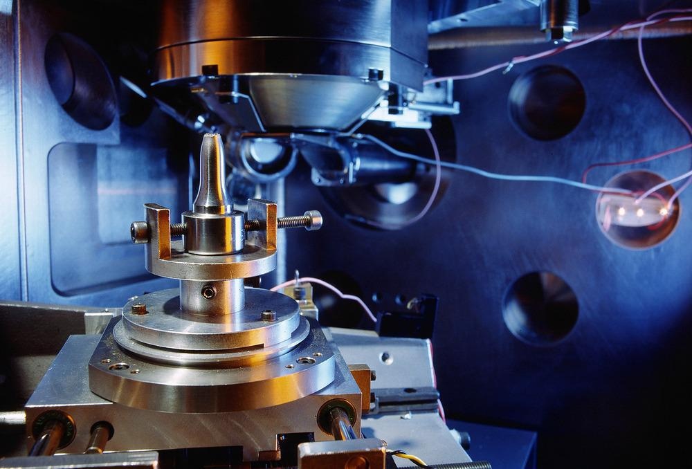
Image Credit: Bildagentur Zoonar GmbH/Shutterstock.com
An Everhart–Thornley sensor detects secondary electrons produced by atoms induced by an electron beam. Samples are examined in an inert atmosphere in a typical SEM. SEM with the nanometer-level resolution is attainable.
The highest resolution attained in SEM is determined by several parameters, including the width of the electron beam and the electron beam's contact area with the material. Some SEMs can attain resolutions of less than 1 nm, yet they cannot approach atomic resolution. Current comprehensive SEMs usually have a resolution of 1-20 nm, although compact devices can have a resolution of 20 nm or higher.
Benefits of Using Electrons Instead of Light in Microscopes
The human eye can detect two points 0.2 mm apart given adequate illumination. This range is called the eye's resolution capability. A lens or lens combination (microscope) can enlarge this range and allow the eye to see objects considerably closer than 0.2 mm apart.
A contemporary optical microscope has a 1000x resolution. Resolving power is restricted by lens quantity and variety, as well as lighting wavelength. White light has a wavelength of 400-700 nanometers (nm), with a mean of 550 nm. This provides a theoretical resolution threshold of the optical microscope of 200-250 nm.
When the wavelength became the significant constraint in optical microscopy, the electron microscope was produced. The wavelength of electrons is substantially shorter, allowing for improved resolution.
Importance of Studying Morphology of Materials
Morphology is the study of shape, structure, and form, which is critical in material science. It is very important for nanoscale materials, also called nanostructures, as shape influences physicochemical characteristics in this situation.
Many research projects necessitate morphological analysis, both descriptive and analytical. Micro- and nanostructures provide a novel way to manipulate biomaterials interfaces. Antibody deposition on particular biomaterial surfaces is greatly influenced by surface characteristics and roughness. The fiber orientation, micro-patterning, and regulated permeability of nanocomposites all have an impact on cellular behavior, causing cellular proliferation, emigration, and development.
The creation of elevated biosensors such as scaffolds for tissue regeneration and drug delivery systems is also influenced by surface morphology and structure. In micro/nano production, surface scanning is used to assess the characteristic design, density, and material defects. For thin-film cells, cross-section imaging can provide thickness information.
Utilization of SEM for Studying Material’s Morphology
Scanning electron microscopy (SEM) is an efficient and useful technique in current materials research, microanalysis, and investigational applications. SEM analysis delivers thorough, high-resolution imaging and elemental mapping features on a broad group of sample types at a diverse range of magnifications. Researchers can also readily acquire elemental composition using an energy dispersive x-ray spectrometer (EDS) connected to a scanning electron microscope (SEM).
Advantages of SEM
There is probably no other equipment that competes with the SEM in the scope of applicability it has in the investigation of bulk objects. The SEM is essential in any field that requires material's morphological characterization as SEMs are rather easy to use, having user-friendly ‘instinctive’ designs. Many applications have a modest amount of specimen preparation. Data acquisition is quick for many applications (less than 5 minutes per image for SEI, BSE, and patch EDS investigations). Modern SEMs yield information in digital formats that are easily transferable.
Limitations of SEM
The microscope chamber must be able to hold solid materials. Vertical measurements are frequently much more limited, rarely exceeding 40 mm. Samples must be maintained in a vacuum of 10-5 to 10-6 torr for most instruments.
Conventional SEM study is not ideal for soluble hydrocarbon-rich materials, wet specimens such as lignite, organic materials, swollen clay minerals, or materials that break down at reduced pressure. Many of the same compounds can be investigated using ‘low pressure’ and ‘environmental’ SEMs.
EDS sensors on SEMs do not identify light elements. Unlike most scanning electron micro-analyzers, which employ wavelength scattering x-ray sensors, most SEMs use solid-state x-ray sensors. Electrostatically insulated materials must be covered with a conductive layer unless the equipment can function in a low vacuum state.
Recent Advancements in SEM
The increased use of SEM in medical studies has been credited with promoting SEM technology improvement. Neuroscience is one field that has propelled this technique forward. SEM is being developed to help tackle previously intractable problems.
SEM has recently advanced in technique and functionality, such as sequential block-face SEM (SBEM), which is used to scan slabs of ultra-thin tissue extracted using an ultramicrotome and then inserted into the scanning electron. In the biological sciences, the invention of FIB-SEM (Focused Ion Beam Scanning Electron Microscopes) signifies another key milestone in SEM technology.
Finally, in recent years, SEM hardware has seen several general improvements. For example, improved lenses and sensors have increased SEM resolution power. These include scanning columns for particle spectrometers, analyzers and lithographs for computer chips, and miniature versions.
References and Further Reading
Vernon-Parry, K. D. (2000). Scanning electron microscopy: an introduction. III-Vs Review, 13(4), 40-44. https://doi.org/10.1016/S0961-1290(00)80006-X
Stoeckel, D., Kübel, C., Hormann, K., Höltzel, A., Smarsly, B. M., & Tallarek, U. (2014). Morphological analysis of disordered macroporous–mesoporous solids based on physical reconstruction by nanoscale tomography. Langmuir, 30(30), 9022-9027. https://doi.org/10.1021/la502381m
Sergeev, Y. M., Spivak, G. V., Sasov, A. Y., Osipov, V. I., Sokolov, V. N., & Rau, E. I. (1984). Quantitative morphological analysis in a SEM‐microcomputer system—I. Quantitative shape analysis of single objects. Journal of microscopy, 135(1), 1-12. https://doi.org/10.1111/j.1365-2818.1984.tb04644.x
Disclaimer: The views expressed here are those of the author expressed in their private capacity and do not necessarily represent the views of AZoM.com Limited T/A AZoNetwork the owner and operator of this website. This disclaimer forms part of the Terms and conditions of use of this website.