Image Credit: Hong Kong University of Science and Technology
This opens the door for photonic integration, which has the potential to transform data communications at a low cost, high volume, high speed, and high throughput.
Photonic integrated circuits, also known as microchips, work with light particles called photons instead of electrons, as in conventional integrated circuits. To expedite data transfer, photonic integration combines electronics and light. This revolution is led by silicon photonics (Si-photonics), which makes it possible to create inexpensive, high-speed connections that can process large amounts of data simultaneously.
While silicon is capable of performing passive optical functions, it is less effective at active tasks like producing light (photodetectors) or detecting it (lasers), which are both essential for the generation and readout of data. For full functionality and increased efficiency, this calls for the integration of III-V semiconductors, which use materials from groups III and V of the periodic table, onto a silicon substrate.
However, even though III-V semiconductors perform well in active tasks, they are not naturally compatible with silicon. Under the direction of Research Assistant Professor Ying Xue and Research Professor Kei-May Lau of the Division of Emerging Interdisciplinary Areas (EMIA), the group set out to solve this problem by figuring out how to effectively use silicon in III-V devices.
They created a unique selective direct epitaxy method known as lateral aspect ratio trapping (LART), which enables the selective growth of III-V materials on silicon-on-insulator (SOI) in a lateral direction without the use of thick buffers.
Their method produced an in-plane III-V laser, which allows the III-V laser to couple with Si in the same plane, which is efficient, even though no integration methods reported in the literature could solve the challenge with high coupling efficiency and high production volume.
Our approach addressed the mismatch of III-V devices and Si. It achieved excellent performance of III-V devices and made it easy and efficient to couple III-V with Si.
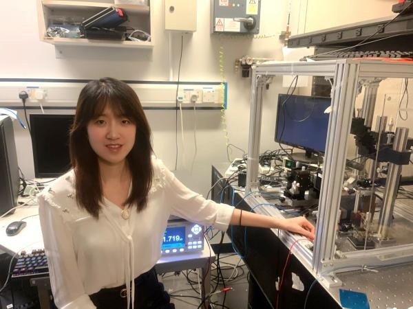
Ying Xue, Research Assistant Professor, Hong Kong University of Science and Technology
Data traffic has increased dramatically over the last few decades due to the rise of new technologies like big data, cloud computing, and sensors. Thanks to Moore's Law, which states that the number of transistors on a microchip doubles roughly every two years, the field of integrated circuits (ICs), also known as microelectronics, has been able to facilitate this growth by producing electronic devices that are faster and smaller. Nonetheless, the limitations of conventional electronic devices have been reached by the ongoing explosion of data traffic.
With the dawn of the Zettabyte Era in 2016, data generation, processing, transmission, storage, and readout saw exponential growth. There are serious issues with speed, bandwidth, cost, and power consumption brought on by this data explosion. This is where Si-photonics, specifically photonic integration, enters the picture.
The team's next steps involve demonstrating the performance of III-V lasers integrated with silicon waveguides, including low threshold, high output power, long lifetime, and high-temperature operation.
Before this method is applied in the real world, she stated that there are important scientific issues that need to be resolved. However, it will make it possible for next-generation communications as well as a number of cutting-edge fields of study and applications, such as supercomputers, artificial intelligence (AI), biomedicine, neural and quantum networks, and automotive applications.
The study was recently published in the journal Laser & Photonics Reviews and selected as cover.
In a related development, Prof. Xue was awarded a grant of US$100,000 by the 2023 Optica Foundation Challenge in recognition of creative solutions for reducing the drawbacks of photonic integrated circuits. Xue plans to use the grant for further research.
Journal Reference:
Xue, Y., et.al (2024) In-Plane 1.5 µm Distributed Feedback Lasers Selectively Grown on (001) SOI. Laser & Photonics Reviews. doi.org/10.1002/lpor.202300549