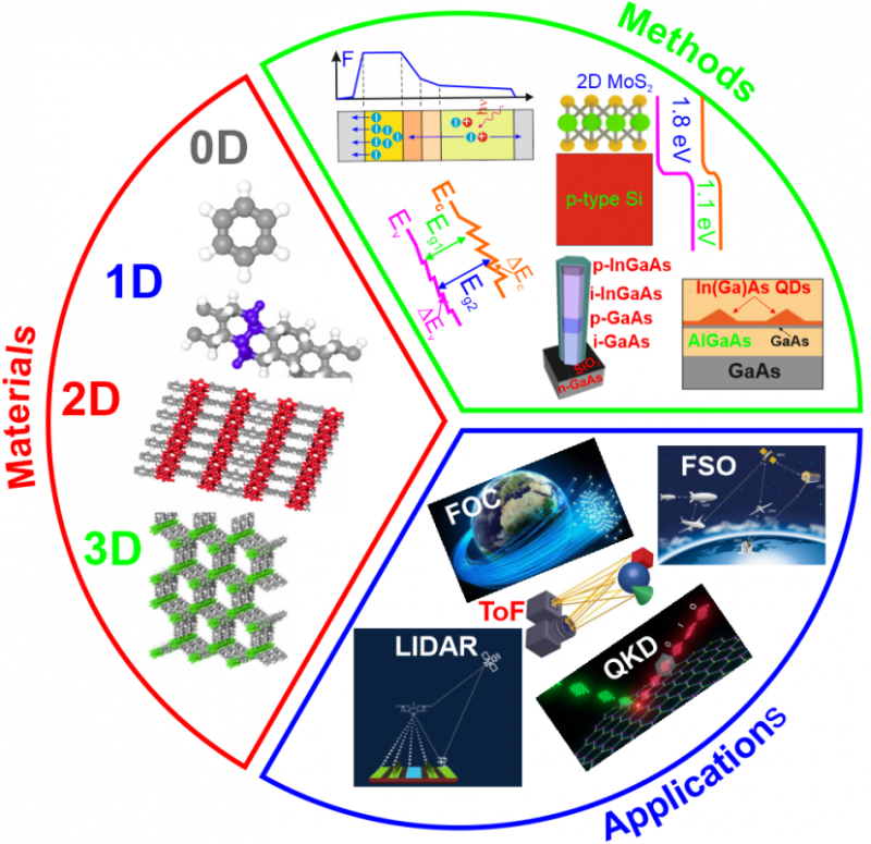
Figure Methods, technologies, and applications roadmap for avalanche photon-sensing technologies starting from bulk to low dimensional materials. Image Credit: Chinese Academy of Sciences
Sophisticated laser radar and weapons systems applied in space and long-range army applications must sense, identify, and monitor different targets under a variety of atmospheric settings that include absorption by CO2, CO, and H2O vapor, resulting in considerable signal attenuation in the optical system.
Besides a system—to properly sense the signal at the detector stage, the output signal suppression needs an additional amplifier. The devices that are dependent on avalanche photodiodes (APDs) featuring high bandwidth (BW) and gain (M)—high gain-bandwidth product (GBW) and low excess noise [F(M)] at the same time—are well matched for sensing suppressed optical signals in the long-range applications like night vision, free-space optical communications (FSO), light detection and ranging (LIDAR/LADAR), time of flight (ToF), intelligent robotic and ultimately in battlefield conditions (military applications).
Undeniably, an important reason for this tendency is the move to optical quantum data applications like quantum key distribution (QKD). Such applications put severe needs on detector performance that go away from the performance of the well-established typical APDs.
Hence, enhancement in GBW and F(M) reduction has been an important target for APD’s advancements. The techniques to suppress the F(M) may be categorized into three tactics. The initial method could be to select a material (to add up “third wave” materials and their methodologies) with beneficial multiplication characteristics. Later, the F(M) might be considerably restricted by scaling the avalanche layer to utilize the non-local effect of the multiplication effect. The final method might be broadly divided as impact ionization engineering (I2E) using rightly designed heterojunctions.
The member of the “third wave” group - two-dimensional (2D) layered materials and their van der Waals (vdW) heterostructures can be utilized in the industry of avalanche multiplication to comprise single-photon counting methodologies. The last ten years have observed an outstanding growth in the number of study papers associated with the potential 2D photodetectors; nevertheless, such materials feature low absorption resulting from a thin atomistic nature. Impact ionization resulting in carrier multiplication is a potential approach to fabricating 2D photodetectors with high detection efficiency.
Compared with standard bulk, the 2D materials feature several outstanding capacities, like strong light-matter coupling, mechanical flexibility, self-passivated surfaces, and gate-tunable Fermi level, offering flexibility in heterostructure design. Such materials are defined by varied impact ionization coefficients versus carrier transport direction.
Besides, in the 2D materials family, both traditional impact ionization and ballistic avalanche mechanisms were noticed. As a result, the study of innovative materials defined by the low critical electric field for avalanche multiplication is important in reaching energy-effective electric/photoelectric devices. In traditional materials, the avalanche multiplication mechanism has been restricted owing to a high driving voltage that could be circumvented by 2D materials-based APDs.
In a new research published in Light Science & Application, a group of researchers, headed by Professor Piotr Martyniuk from the Institute of Applied Physics, Military University of Technology, Poland, and co-authors from State Key Laboratory of Infrared Physics, Shanghai Institute of Technical Physics, Chinese Academy of Sciences, China have displayed existing status and future development on IR-based APDs. The research includes bulk HgCdTe, as well as AIIIBV-based material systems along with well-recognized “third wave” material family member—superlattices.
Besides, the existing advancement in the new materials and architectures for high-performance IR APDs was presented to comprise breakthrough “third wave” 2D materials. Additionally, the strategies to attain high-performance APDs are shown.
Journal Reference
Martyniuk, P., et al. (2023). Infrared avalanche photodiodes from bulk to 2D materials. Light: Science & Applications. doi.org/10.1038/s41377-023-01259-3