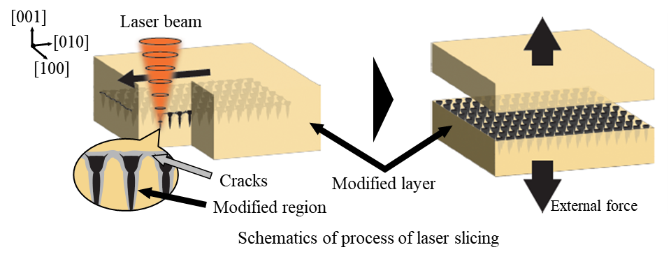
Focusing the energy of a laser beam into a small volume of a diamond sample creates tiny ‘modified regions.’ If these modified regions are laid out in a precise grid-like pattern, the ensuing cracks make it easy to separate a {100} wafer from the diamond. Image Credit: Hirofumi Hidai from Chiba University
As far as the semiconductor industry is concerned, diamonds are promising materials, but slicing them into thin wafers is difficult. In a recent study, a research group from Chiba University developed a novel laser-based method for easily slicing diamonds together with the optimal crystallographic plane.
Their study outcomes will help make diamonds affordable semiconductors for highly effective power conversion in electric vehicles and also for high-speed communication technologies.
At present, silicon-based materials are known to be the unchallenged leaders in semiconductors. Still, researchers across the globe have been actively trying to identify excellent alternatives for next-generation electronics and high-power systems.
Fascinatingly, diamonds come under the most promising materials for applications like quick telecommunications and power conversion in power plants and electric vehicles.
Despite their appealing properties for the semiconductor industry, the applications of diamonds are limited as a result of the lack of a method to slice them into thin wafers in an efficient manner. Consequently, diamond wafers should be synthesized one by one, thereby making fabrication charges prohibitive for the majority of industries.
A research group from Japan, headed by Professor Hirofumi Hidai from the Graduate School of Engineering at Chiba University, has found a solution to this problem.
In a recent study, a novel laser-based slicing method could be utilized to neatly slice a diamond together in the optimal crystallographic plane, thus generating smooth wafers.
The study was available online on May 18th, 2023, and reported in the journal Diamond & Related Materials on June 2023.
Master’s student Kosuke Sakamoto has co-authored their study from the Graduate School of Science and Engineering at Chiba University with former Ph.D. student Daijiro Tokunaga, presently an Assistant Professor at the Tokyo Institute of Technology.
The properties of the majority of the crystals, such as diamonds, change along various crystallographic planes—imaginary surfaces containing the atoms, including the crystal. For example, a diamond could be sliced easily along the {111} surface. But slicing {100} is difficult since it also produces cracks together with the {111} cleavage plane, increasing kerf loss.
To avoid the propagation of such unwanted cracks, the scientists came up with a diamond processing method that concentrates short laser pulses onto a narrow cone-like volume inside the material.
Concentrated laser illumination transforms diamond into amorphous carbon, whose density is lower than that of diamond. Hence, regions modified by laser pulses undergo a reduction in density and crack formation.
Hirofumi Hidai, Professor, Chiba University
By shining such laser pulses onto the transparent diamond sample in a square grid pattern, the scientists made a grid of small crack-prone regions within the material.
If the space present between the altered regions in the grid and various laser pulses utilized per region are optimal, all altered regions link to each other via small cracks that preferentially propagate together with the {100} plane.
Accordingly, a smooth wafer with {100} surface could be easily isolated from the rest of the block by just pushing a sharp tungsten needle against the sample’s side.
In general, the suggested method is a pivotal step toward making diamonds an ideal semiconductor material for future technologies.
Diamond slicing enables the production of high-quality wafers at low cost and is indispensable to fabricate diamond semiconductor devices. Therefore, this research brings us closer to realizing diamond semiconductors for various applications in our society, such as improving the power conversion ratio in electric vehicles and trains.
Hirofumi Hidai, Professor, Chiba University
Journal Reference
Sakamoto, K., et al. (2023) Laser slicing of a diamond at the {100} plane using an irradiation sequence that restricts crack propagation along the {111} plane. Diamond and Related Materials. https://doi.org/10.1016/j.diamond.2023.110045.