For instance, photonic integrated circuits are hatching as a promising candidate to revolutionize conventional integrated electronic circuits for its exceptional advantages such as broad bandwidth, high operation speed, and low power consumption. Nevertheless, as the most fundamental building block of integrated photonics, conventional optical waveguides still encounter challenges in terms of bulk footprint, compromised light-matter interaction efficiency, and restrained available functionalities. Fortunately, the concept of meta-waveguides can be adopted here to open a new avenue towards powerful manipulation of guided light in subwavelength scale, infusing new degrees of freedom into waveguide landscapes to dramatically boost device performance and enable novel functionalities.
In a new paper published on the journal of ‘Light: Science & Applications’, a team of scientists from China, United States and Italy have presented a comprehensive review article offering a panorama on the optic of meta-waveguides. Latest advances on various subwavelength meta-structured waveguides are systematically cataloged, encompassing a broad class of photonic devices and systems that ally metamaterials and metasurfaces with diverse optical waveguides (dielectric/ plasmonic/ optical fibers). Brief physical fundamentals with explicit design methods (including both forward and inverse design tutorials) and representative applications for meta-waveguides are comprehensively summarized. The authors highlighted “how incorporating the concepts of meta-optics with waveguide technologies can propel photonic integrated circuits into new heights, by providing versatile efficient coupling interfaces, novel on-chip optical signal processing paradigms and diverse platforms for sensing, imaging and artificial intelligence”.
Figure 1 briefly introduces the zoology of meta-waveguide family. A plethora of applications are prototyped on this flexible playground, including, for instance, metasurface-patterned dielectric waveguides, forward designed metamaterial waveguides, metasurface- or metamaterial-hybrid optical fibers, meta-structures- assisted plasmonic waveguides, and inverse designed metamaterial waveguides, to name a few.
As illustrated in Figure 2a, meta-waveguides can be classified via either design methods or underpinning waveguide platforms.
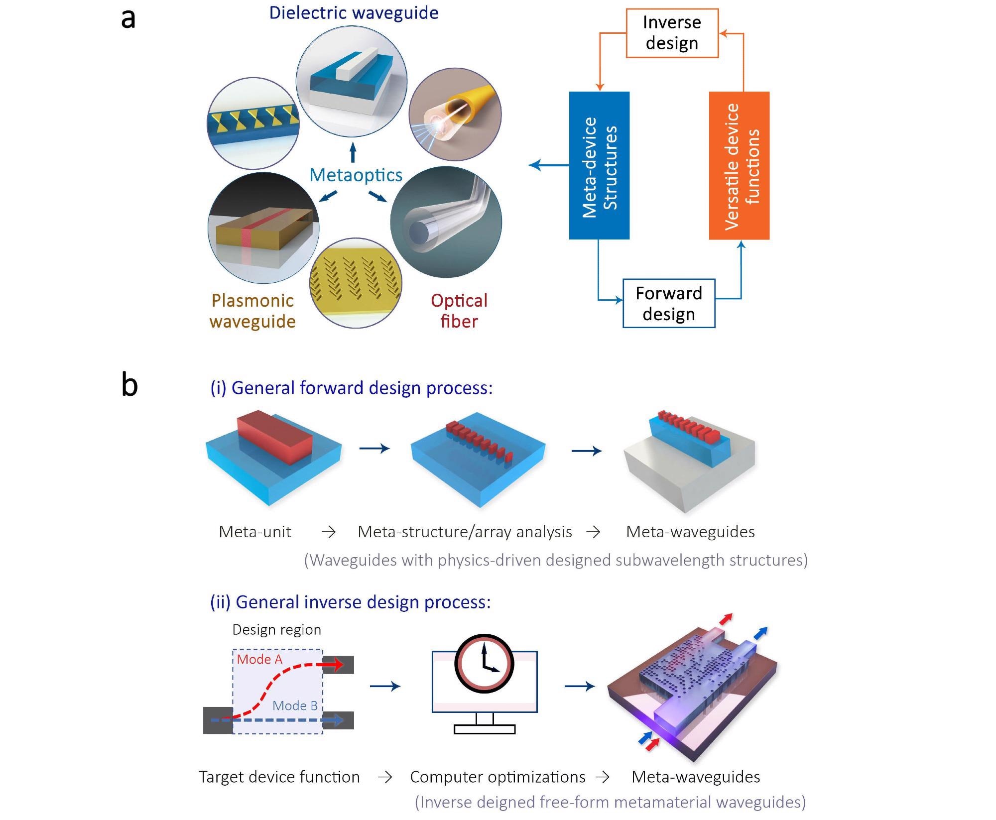
Figure 2. Meta-waveguide attributes. a, if classified by design method, meta-waveguides can be conceived either by physics intuition-based forward design or computer optimizations-based inverse design. If categorized by waveguide platforms, meta-optics can be saddled with dielectric waveguides, optical fibers and plasmonic waveguides. b, Two general directions to design meta-waveguides: physics intuition-based forward designs and inverse design methods. Image Credit: Yuan Meng, Tsinghua University
“On the one hand, meta-waveguides can be conceived by physical intuition-based approaches (namely forward design henceforth) by leveraging the toolbox of metasurfaces and metamaterials with waveguide optics.”
“On the other hand, we can also use inverse design, which relies on computer optimizations (see Figure 2b), to develop free-formed analog (curvilinear boundaries) or digital (with relatively regular boundaries) metamaterial waveguides.”
Photonic structures with subwavelength details are canonical to meta-waveguides. Taking two-dimensional periodic silicon segments as an instance, the meta-waveguides should be modeled as a designer effective medium, which is different from the photonic bandgap theory found in photonic crystals or scalar diffraction theory used in non-subwavelength gratings.
“Despite the concept of meta-waveguides is still in its infancy, exciting progress are hatching with bright perspectives and profound potential applications. As conceptually illustrated in Figure 3, the advancement of meta-waveguides can not only extend meta-optics to the realm of guided electromagnetic waves and waveguide technology, but also promise to reshape the landscapes of photonic integrated circuits and massive emergent applications,” as the scientists envisaged.
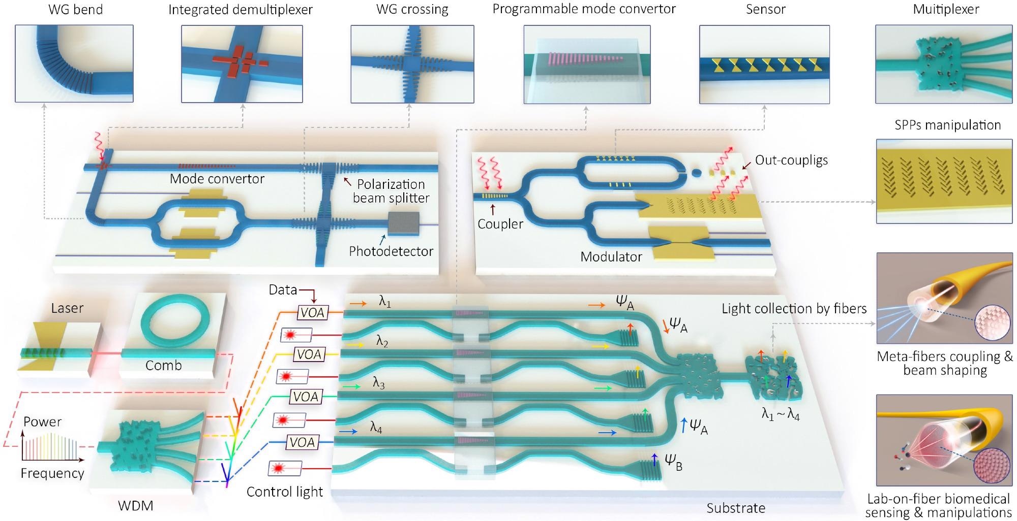
Figure 3. Outlook on photonic integrated “meta-circuits”. Diverse meta-waveguide-based photonic devices can be competitive substitutes for conventional integrated optical scenarios with compact footprint, enhanced efficiency and multifunctionality. Image Credit: Yuan Meng, Tsinghua University
Meta-waveguides may further venture photonic integrated circuits and many relevant applications in biomedical sensing, imaging, and detection into new territories. Massive novel emerging device functions will still await exploring in this vibrant field.