Sponsored by MKS OphirReviewed by Olivia FrostAug 4 2026
Displays are common in modern life, from tiny displays inside AR/VR gear just in front of the user’s eyes to large TV screens and monitors viewable at a distance. Display technology has advanced considerably from the days of bulky cathode ray tubes, with flexible and transparent OLED displays now leveraging light-emitting organic molecules.
Image Credit: CeltStuido/Shutterstock.com
As new technologies become more prominent, equipment suppliers must closely track trends and opportunities, with OLED and microLED technologies gradually replacing LCD (liquid crystal display) technology. The laser industry is no exception, with lasers now seeing increasing use in OLED and microLED display manufacturing.
Understanding Display Technologies
LCD is a transmissive technology, meaning that the pixels’ function is to block or pass light generated behind them. The on/off function is achieved by applying a voltage to a thin layer of liquid crystal held between two polarizers.
OLED and microLED are emissive technologies, meaning that each individual pixel is a small light source. OLED pixels are based on light-emitting organic molecules, while microLED pixels are semiconductor LEDs.
OLED molecules are directly deposited on the display backplane, while microLED chips are manufactured on a semiconduction wafer and transferred onto the backplane. This technology has already seen widespread adoption in the market, but microLED is seeing slower uptake despite offering several advantages.
The key challenge hindering the more widespread adoption of microLED technology is the process of transferring individual microLED pixels from the semiconductor wafer onto the final display product’s backplane.
Table 1 highlights the differences between these technologies.
Source: MKS Ophir
| |
LCD |
OLED |
microLED |
| Response time |
ms |
μs |
ns |
| Viewing angle |
Narrow |
High |
High |
| Power efficiency |
Medium |
Medium |
High |
| Flexible display |
No |
Yes |
Yes |
| Brightness |
Medium |
Low-medium |
High |
Laser Applications in OLED Display Manufacturing
The process of manufacturing an OLED display is typically divided into three stages:
- Deposition and crystallization of amorphous silicon to create the pixels’ conductive wiring
- Pixel formation, including the red-, green-, and blue-emitting OLED molecules that must be deposited via ink-jet printing or vapor deposition
- Encapsulation and lift-off
Encapsulation is particularly challenging, because OLED molecules are highly sensitive to moisture. The display must be encapsulated between thin layers of polymer or glass while ensuring this is kept moisture-free.
Lift-off also poses specific challenges. OLED displays are manufactured on transparent polymer sheets, with the display resting on a glass substrate that supports it during the fabrication process. The display is ‘peeled’ off the glass once it is ready: this process is referred to as ‘lift-off.’
Lasers are used in a range of OLED display manufacturing steps.
- Laser Annealing: Laser annealing transforms amorphous silicon into polycrystalline silicon. The laser beam’s energy allows the silicon atoms to move around until they eventually settle into a stable crystallized form.
- Laser Lift-Off: Lasers can be used to separate the OLED display from the glass substrate. This is achieved by forming the laser beam into a narrow, thin line that scans across the OLED display. The laser beam is then absorbed at the interface between the OLED display and the glass interface, separating the two components.
- Cutting and Drilling of Polymer and Glass Parts: Laser-based cutting and drilling are achieved by evaporating material rather than removing it, for instance, with a drill. This approach allows thin, fragile materials to be processed without cracking.
Laser Applications in microLED Display Manufacturing
microLED pixels are manufactured using a traditional semiconductor process, meaning that they must then be transferred onto the microLED display backplane.
This transfer is currently the most challenging step in microLED manufacturing. For example, a microLED TV screen requires that millions of micron-sized microLEDs be accurately and rapidly transferred from the wafer onto the display backplane.
The microLEDs are much denser on the semiconductor wafer than on the display, further complicating this process and making it impossible to transfer groups of microLEDs simultaneously.
A number of organizations are developing technologies designed to make this transfer step more efficient. For example, Uniqarta has developed a technology that employs a rapidly moving laser beam to selectively release microLED chips from a polymer carrier onto the display backplane.
MicroLED chip release is achieved by locally heating the polymer carrier, triggering its expansion and generating a ‘bump’ that pushes the microLED chip away.
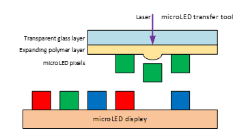
MicroLED transfer using laser-induced expansion of polymer. Image Credit: MKS Ophir
Lasers Suitable for OLED and microLED Manufacturing
Two types of pulsed UV lasers are commonly employed in OLED and microLED display manufacturing: excimer lasers and solid-state lasers.
Excimer lasers emit in the UV range, using a halogen-noble-gas compound. Solid-state lasers use diode lasers to pump a crystal, or they employ a fiber that has been doped with rare earth elements such as neodymium, which is able to emit in the near IR.
Additional crystals can be employed to double or triple the frequency, while other components can be used to control the pulse width down to the femtosecond range. Table 2 shows typical parameters of excimer and solid-state lasers.
Source: MKS Ophir
| |
Excimer |
Solid state |
| Wavelengths |
193 nm, 248 nm, 308 nm |
1030–1070 nm fundamental harmonic
515–535nm, second harmonic
343–355, third harmonic |
| Pulse width |
ns |
ns, ps, fs |
| Repetition rate |
kHz |
kHz-MHz |
| Average Power |
Up to ~1 KW |
Up to ~200 W |
| Pulse energy |
mJ–J |
μJ–mJ |
Excimer lasers offer more power, but this is not the only essential parameter when looking to increase throughput. For example, pulse width also plays a key role, and as the pulse becomes shorter, the instantaneous power for a given pulse energy increases.
These high instantaneous laser powers cause the material to be vaporized before heat can flow outside the intended work area, so this heat is not wasted and does not have the opportunity to cause damage.
This approach is occasionally referred to as ‘cold processing’ because it is possible to cut through glass without heating it. A process requiring 1000 W with a nanosecond laser may therefore require far less power with a femtosecond laser.
Most applications require UV lasers, but some do use visible and IR lasers. These include:
- Heating solder for removing a defective microLED and soldering a new microLED in its place
- Patterning the fine metal mask used in OLED
- Cutting ultra-thin glass
Measuring the power of these lasers is a significant challenge. Selecting the ideal laser sensor depends on average power and power density (kW/cm2), but energy density (J/cm2) must also be considered for pulsed lasers.
Short-pulse lasers in the picosecond and femtosecond range may have relatively low power and energy density, but there is still a risk of damage to general-purpose sensors due to these lasers’ extremely high instantaneous power.
This is particularly true for UV lasers, because the photon energy of these lasers is high and photons can more easily break molecular bonds. It is imperative that the right sensor be tailored to the application.
Acknowledgments
Produced from materials originally authored by Dr. Efi Rotem from Ophir Photonic Group.

This information has been sourced, reviewed, and adapted from materials provided by MKS Ophir.
For more information on this source, please visit MKS Ophir.