LiDAR (light detection and ranging) is the optical equivalent of radar. LiDAR, as an active sensor that acquires 3D information, plays critical roles in remote sensing, defense, and autonomous driving.
A LiDAR is made up of three major modules: transmitting, beam steering and receiving. It measures the distance between targets by illuminating them with laser signals of specific wavelengths, and it obtains additional 3D information by mechanically or electromagnetically scanning the target’s surface.
The ToF ranging principle, which modulates laser beams in the time domain, is a popular LiDAR distance measurement method. The emitter sends a laser pulse to a target, and the receiver acquires the reflected laser pulse. ToF measures range by counting the round-trip flight time of laser pulses emitted between the LiDAR and the target.
Timing is essential for ToF LiDAR distance measurement; its precision is critical to the LiDAR’s ranging precision. A TDC is used to measure the time interval between the emission and arrival of laser pulses to get the correct timing. TDC is a chip that counts the time between start and finish signals and reverts it to the measurable digital medium.
A time–analog and analog-to-digital converter can quantify time intervals down to the picosecond range and transform time intervals from analog signal to digital signal.
The two main implementation methods are ASIC-based TDC realization and FPGA-based TDC realization.
The goal of a recent paper was to illustrate a low-cost digitally integrated LiDAR with TDC that is completely FPGA-controlled and processed in a low-end FPGA chip with constrained configurable logic block resources.
Numerous MCU and ASIC chips are needed for a LiDAR system to realize the control and processing features of a 2D LiDAR, such as pulse control, motor control, ToF calculation, and data processing.
An FPGA, with its ability to perform parallel and simultaneous processing, can realize high-speed computation in the form of a low-cost coprocessor. The logic functions of a 2D LiDAR are integrated into a single low-end FPGA in this paper.
Methodology
The ToF spanning principle is to quantify the travel time of particles or waves between the emitter and the target. Counting clock pulses is the most basic method for determining the time interval between two events.
The pulse counting method works based on calculating the number of system clock signals produced by the IHIT signal during its valid time. It is simple to implement in an FPGA by starting and finishing a counter.
Figure 1 depicts the delay line’s operating principle. The delay line is made up of several delay cells and a D-type flip-flop (FFD) array. These delay cells are connected in a series to form a tapped delay line. The start signal is infused from the delay line’s head and continues to perpetuate in a specific direction along the entire line. The state of the delay tap in binary adjustments each time the signal passes through a delay cell.
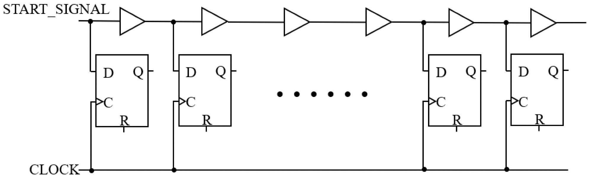
Figure 1. The architecture of the delay line. Image Credit: Huang, et al., 2022
The fast carry logic with the peek element is CARRY4, which is situated in the slice of the configurable logic block and can be used as the time interpolator to construct the tapped delay line. Figure 2a represents a simple schematic of CARRY4 in FPGA.
Each CARRY4 cell is made up of four multiplexers (MUXCY) and four XOR gates. Port CI is the start signal’s input, and port CO3 is the delay line’s output. A long delay line is formed by cascading several CARRY4 cells into an array. Figure 2b depicts the use of CARRY4 cells in delay line logic.
The time resolution of the FPGA-TDC is calculated by the time interval of the signal crossing a delay cell, which is similar to the time needed for signal propagation from Cl to CO3.
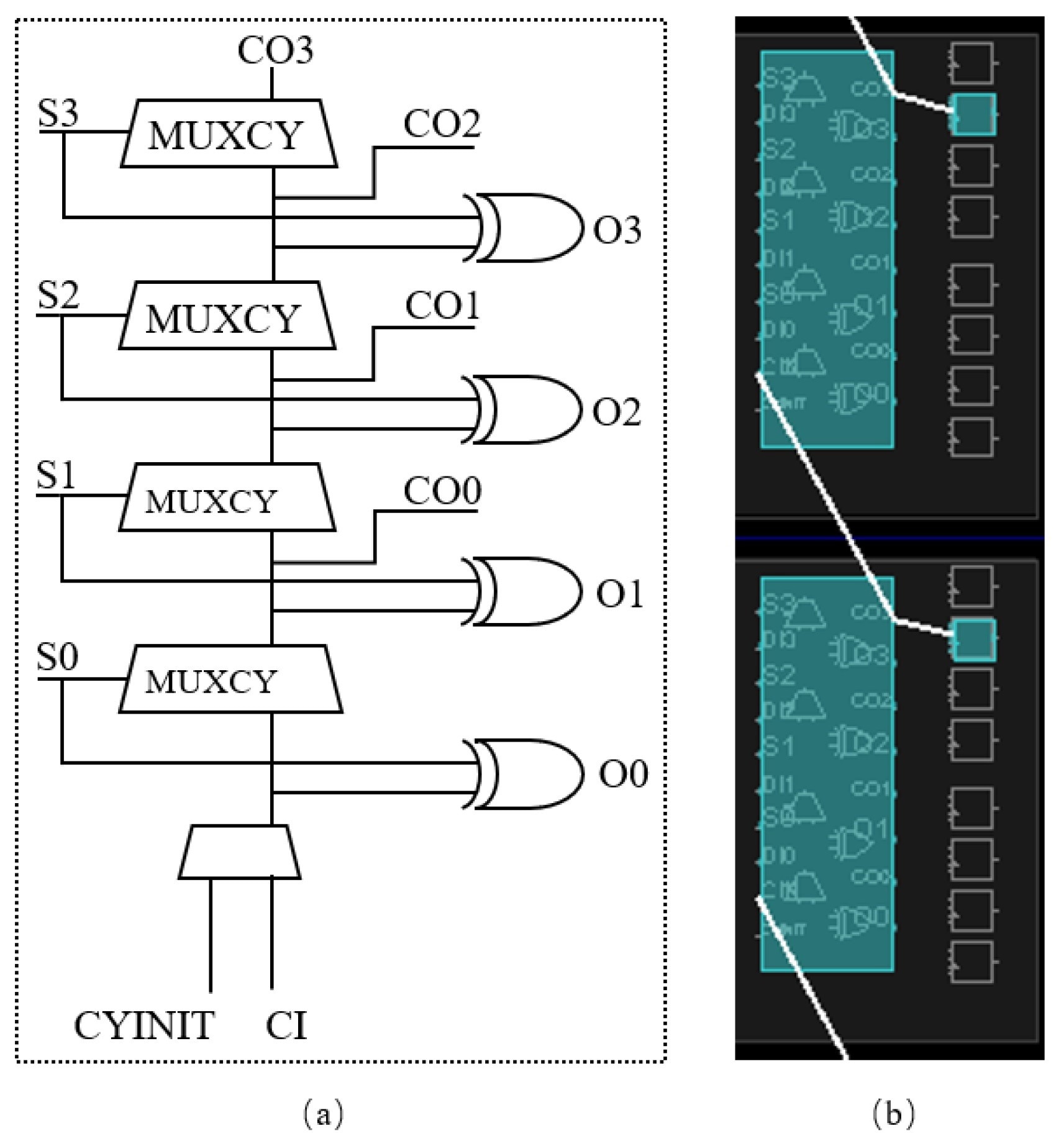
Figure 2. (a) CARRY4 elements in Xilinx FPGA; (b) delay line structure. Image Credit: Huang, et al., 2022
Figure 3 depicts the time measurement procedure. The start signal is at a high logical level in the beginning, and the coarse counter begins to work concurrently. The fine counter is stimulated when the stop signal is powered up.
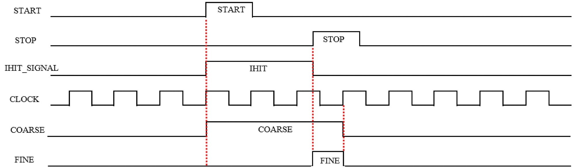
Figure 3. Fine and coarse time measurements. Image Credit: Huang, et al., 2022
Results and Discussion
When the input signal is greater than the system clock, it is essential to narrow it while keeping the delay line engaged within one system clock. As a result, the delay line could acquire one available conversion value per input signal from a pool of possible input signals. Figure 4 depicts the input filter schematic and simulation results.
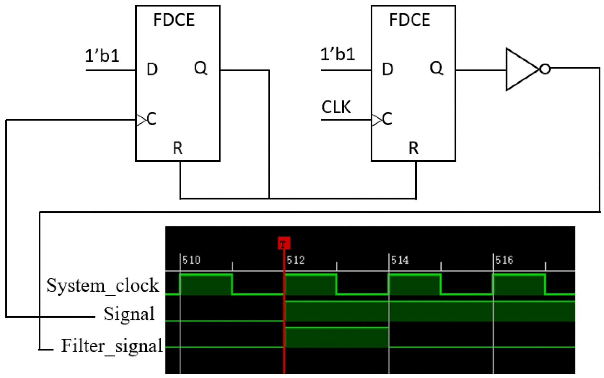
Figure 4. Input filter schematic and simulation result. Image Credit: Huang, et al., 2022
A ZYNQ-7010 (XC7Z010) SoC was used to implement the proposed FPGA-TDC. Figure 5a depicts the proposed TDC implementation block diagram.
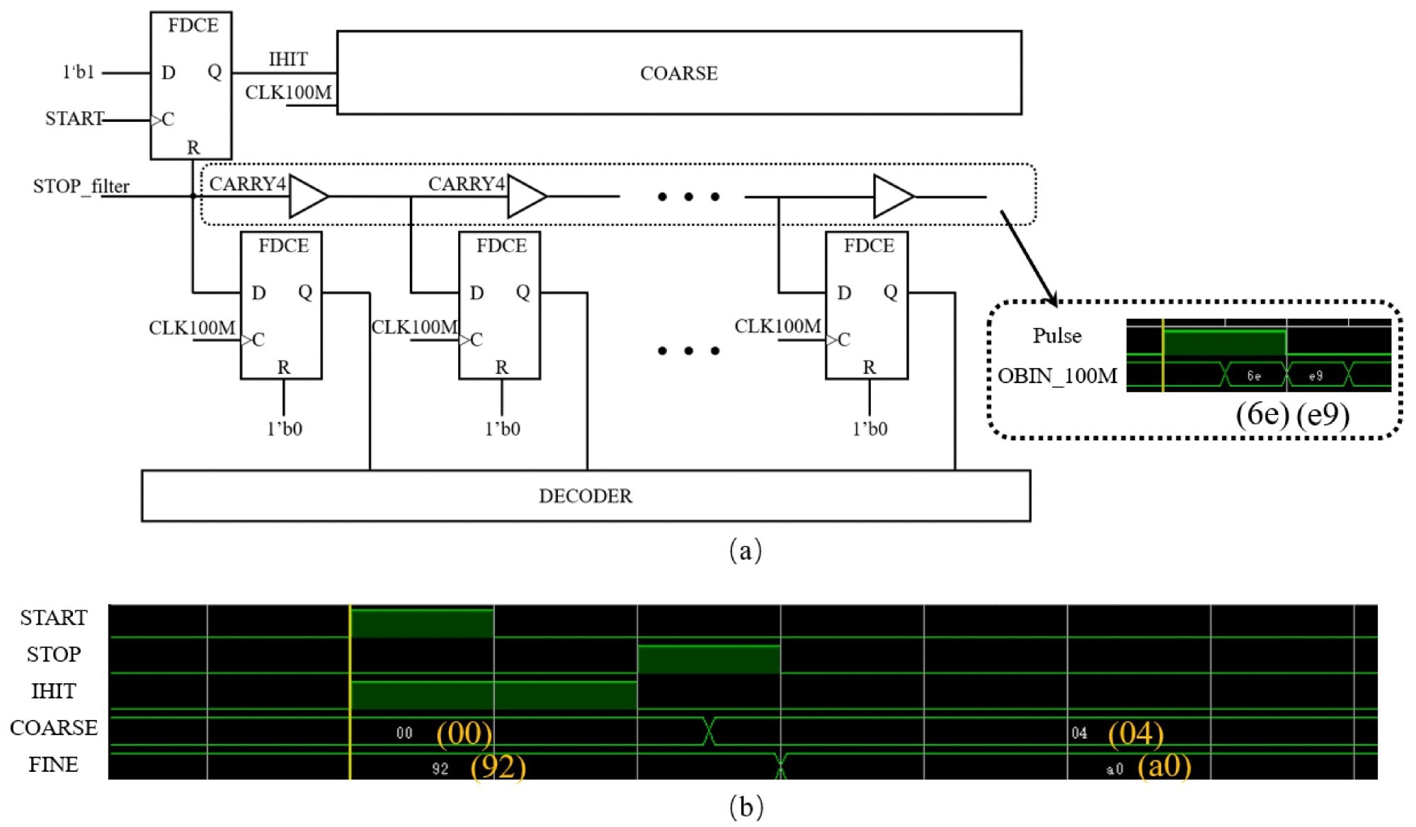
Figure 5. (a) Block diagram of TDC and average LSB simulation; (b) TDC timing simulation. Image Credit: Huang, et al., 2022
Figure 5b depicts the FPGA-TDC simulation results, such as the start, stop, and IHIT signals, coarse time, and a fine time. The IHIT signal is fully defined by the rising edges of the start and stop signals.
The coarse counter acquires the measurement value when the stop signal arrives. The fine value was calculated when the next rising edge of the system clock arrives. By incorporating the coarse and fine counters, the exact time interval is derived.
The semiconductor fabrication procedure and external factors have an impact on the TDC’s LSB. The differential nonlinearity (DNL) function is used to analyze the LSB difference between both the converted and ideal values, and the integral nonlinearity (INL) is the DNL accumulation sum. DNL and INL are determined using a standard code density test method and bin-by-bin calibration.
The technique works on the principle of generating a large number of external random pulses as the TDC input and recording the times of each delay cell. The statistical code measurement is used to assess the overall resolution. Each time, the counting result is saved in the system’s random access memory (RAM). Figure 6 depicts the RAM setup process.
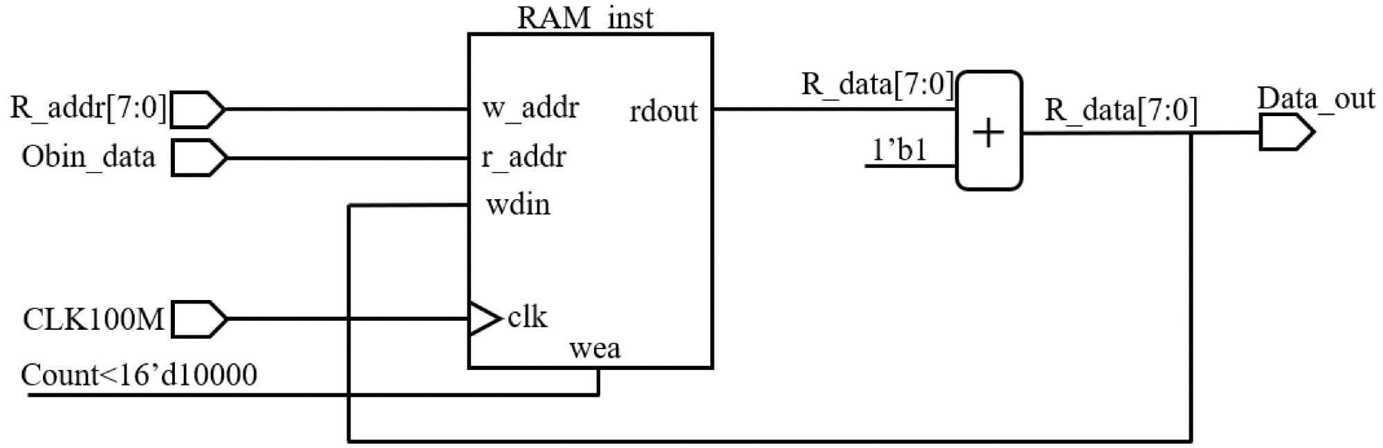
Figure 6. Code density statistics diagram. Image Credit: Huang, et al., 2022
After around 10,000 points were collected, the hit pulse injection was stopped, and a PC for data analysis perused the values of each address in RAM out. Figure 7a depicts the statistical data of each carry series.
The DNL and INL were evaluated over the full range of the delay line in the TDC after bin-by-bin calibration and acquired through the code density test. Figures 7b and c show the results: the DNL is within 1 LSB and the INL is within 2.5 LSB.
Furthermore, excessive resource utilization in an FPGA hurts the layout and wiring inside, causing the system to become more unstable. Figure 7d summarizes the source utilization in the FPGA after synthesis and implementation.
Table 1 shows the resource utilization in full configuration, where only 2112 DFFs, 1056 LUTs, and 8 IO ports are used. These results demonstrate that the proposed TDC uses few resources. Table 2 shows the energy consumption of the FPGA-TDC, which is very low.
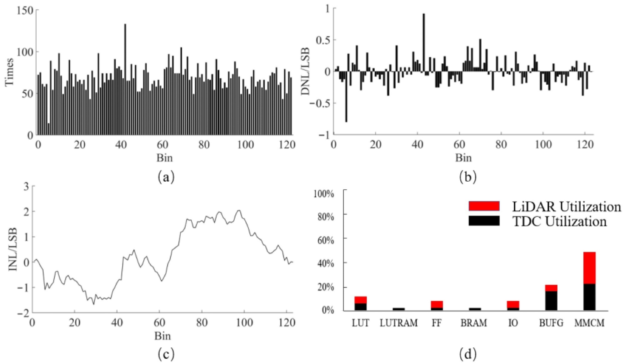
Figure 7. (a) Statistical analysis of the TDC bins; (b) DNL; (c) INL; (d) FPGA resource utilization. Image Credit: Huang, et al., 2022
Table 1. The TDC resource utilization. Source: Huang, et al., 2022
| Resource |
Used |
Utilization |
| LUTs |
1056 |
6% |
| DFFs |
2112 |
6% |
| IO |
8 |
6% |
Table 2. Power consumption. Source: Huang, et al., 2022
| Name |
Consumption |
| Dynamic |
0.193 W |
| Clocks |
0.029 W |
| Signals |
0.038 W |
| Logic |
0.031 W |
| MMCM |
0.095 W |
| I/O |
<0.001 W |
| Total |
0.288 W |
When contrasted to some initially published works using TDL techniques, the FPGA-TDC has a limited resource cost, as shown in Table 3.
Table 3. Comparison of resource utilization. Source: Huang, et al., 2022
| Work |
Utilization (LUTs, DFFs) |
| This paper |
1056, 2112 |
| [24] |
3837, 7010 |
| [21] |
>2000, >2000 |
A pulsed laser diode (LD) is small in volume, with a high peak power and conversion rate. Figure 8 shows the driver circuit schematic—the laser diode is an Osram SPL PL90-3 at 905 nm wavelength from Munich, Germany. The LD requires a small trigger and energy storage to achieve high peak power.
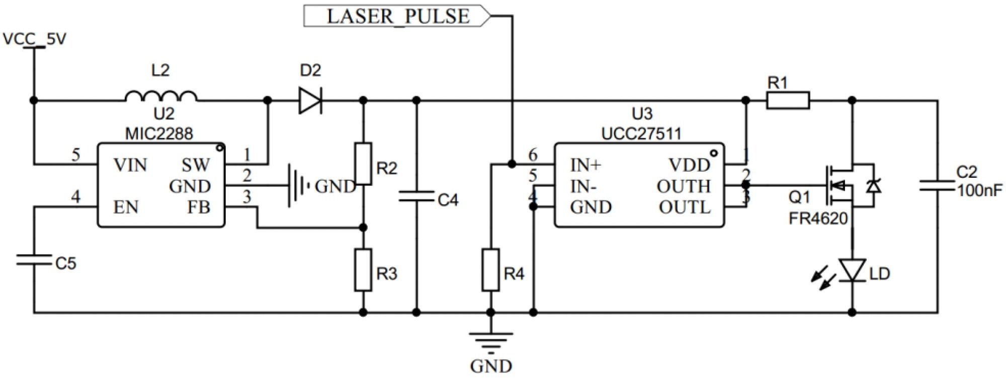
Figure 8. Laser drive circuit. Image Credit: Huang, et al., 2022
Figure 9a depicts the circuit schematic. The DC-DC boost circuit shown in Figure 9b offers a high reverse voltage.
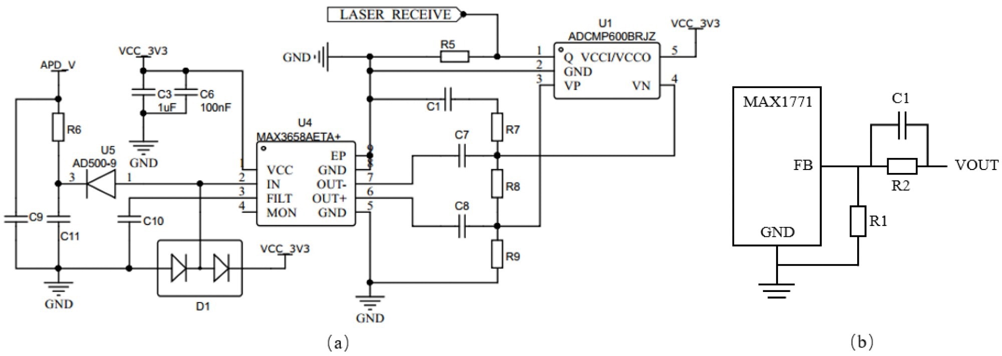
Figure 9. (a) Receiver circuit. (b) Bias voltage circuit. Image Credit: Huang, et al., 2022
Figure 10a depicts the transceiver module’s printed circuit board (PCB).
More precise measurements are possible with symmetrical transmitting and receiving lenses. This module incorporates the laser transmitting and receiving circuits, which are both fueled by the 5 V DC power supply. To cut power supply requirements, all components in the LiDAR prototype distribute a 5 V DC power supply.
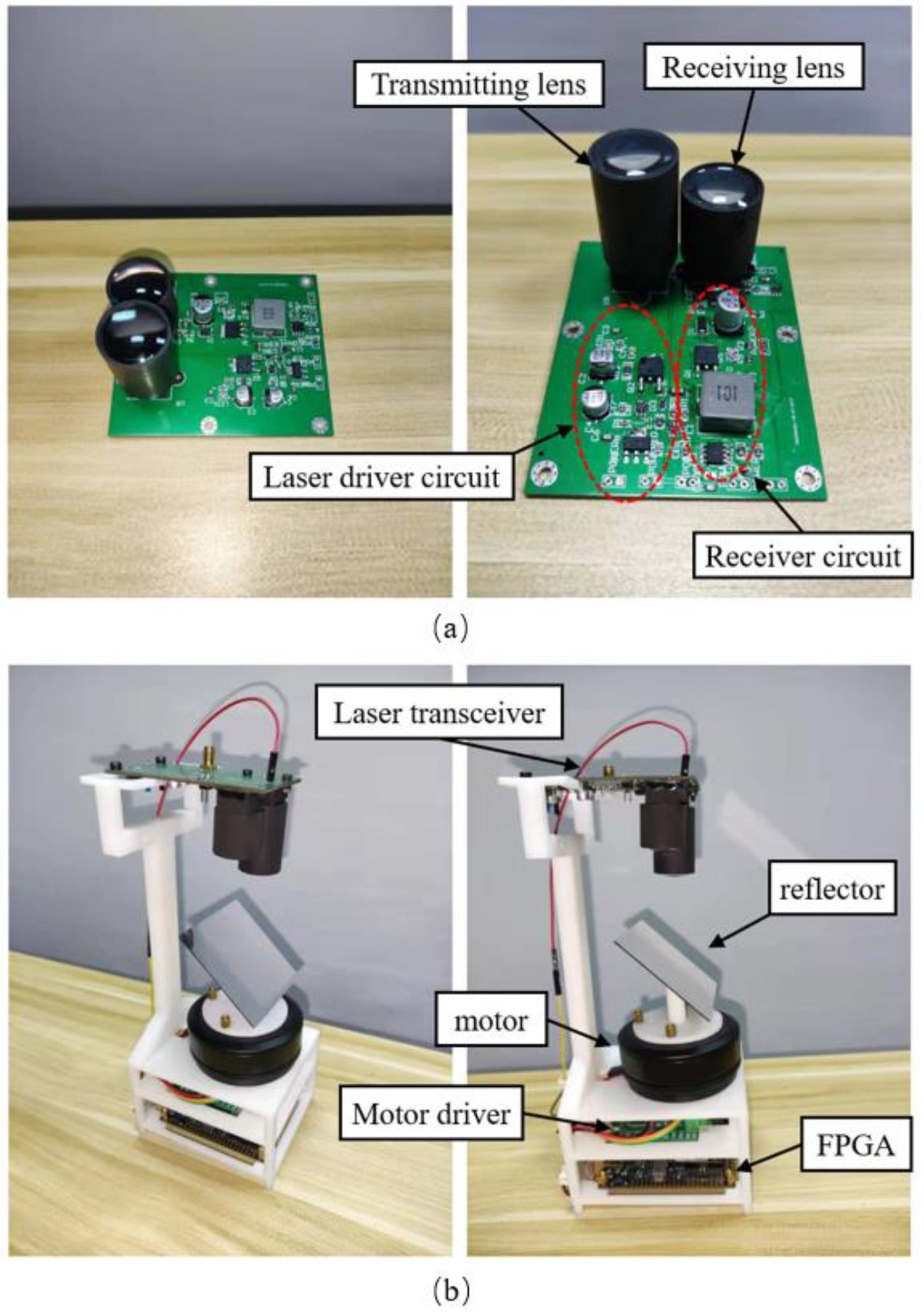
Figure 10. (a) Laser transceiver module. (b) The prototype of the 2-D LiDAR system. Image Credit: Huang, et al., 2022
As shown in Figure 10b, the presented LiDAR system primarily consists of a motor, a reflector, an FPGA controller, and a laser transceiver module.
An infrared camera and an oscilloscope were used to test the laser spot size and pulse waveform. The laser spot, recorded by the infrared camera, is shown in Figure 11a, where it is collimated through a 38 mm lens. At a distance of 2 m, the laser spot has a diameter of about 3 cm.
The oscilloscope captures and visualizes the FPGA trigger signal (top) and the distributed pulse signal (bottom) in Figure 11b.
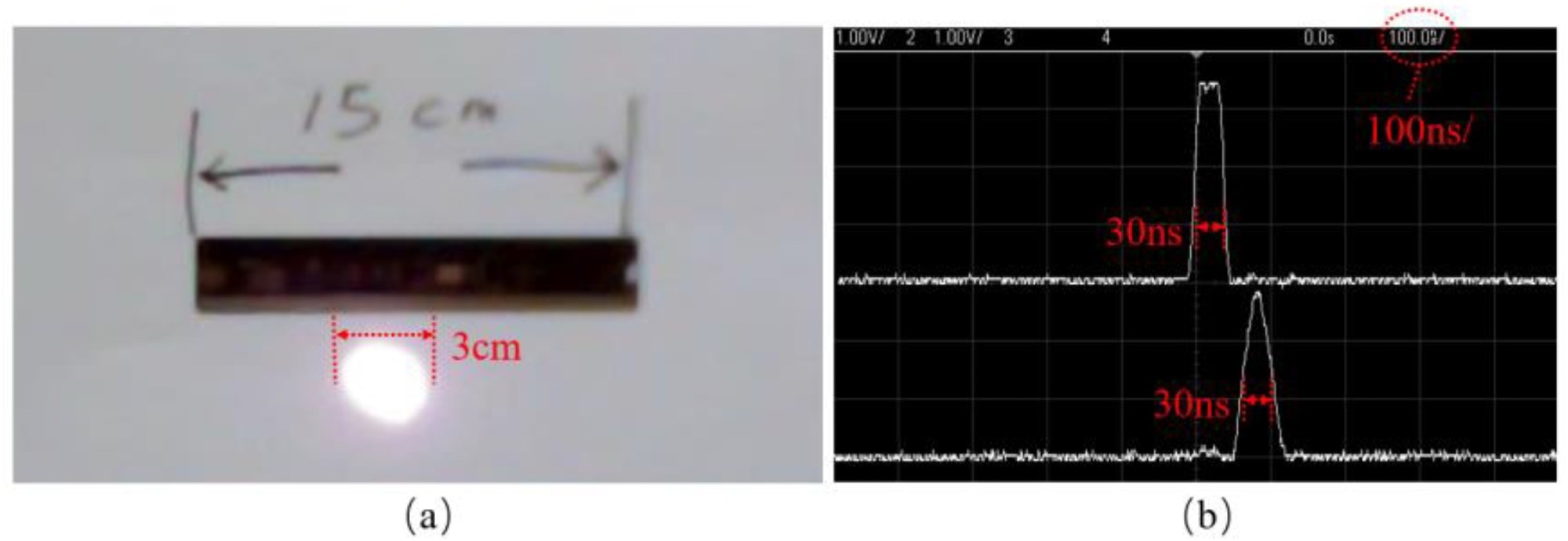
Figure 11. (a) Laser spot. (b) The waveforms of the trigger signal and transmitter pulse. Image Credit: Huang, et al., 2022
After many measurements, the LiDAR’s ranging data were adjusted and tested at 1.5 m and 3 m distances, as shown in Figure 12a. For each distance, 2000 points were evaluated, and almost all of them were very close to the true distance, demonstrating the timing and ranging precision.
Figure 12b depicts the deviation—most of the points are very close to the ground truth distance with very little deviation, indicating a distance measurement precision of around 0.02 m.
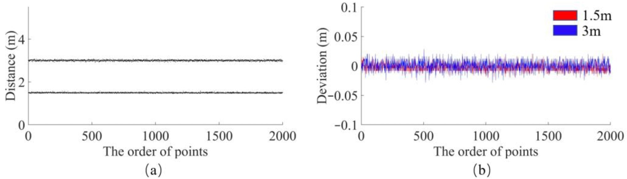
Figure 12. Ranging test. (a) Distance test of 1.5 m and 3 m; (b) Deviation test of 1.5 m and 3 m. Image Credit: Huang, et al., 2022
Following that, targets with complex profiles and wide-view scanning were evaluated to validate the 2-D LiDAR’s ranging and scanning effectiveness. The frequent improvements of the obstacle edge in the horizontal direction are good targets for assessing the LiDAR.
One scanning clearly distinguishes the horizontal profile of the object in Figure 13a. The edge distance between the box and the wall is distinct and divergent.
An object with constant shape changes in the horizontal profile was evaluated in Figure 13b. The target contour is detailed and has almost no distortion when contrasted with the image.
Furthermore, wide-view scanning was evaluated, and the result, as shown in Figure 13c, revives the distance profile of the surroundings in the image. Figures 13d and e show the scanning outcomes of a wall corner and an obstacle with a round shape. On the right side of Figure 13, the distance between each point is depicted.
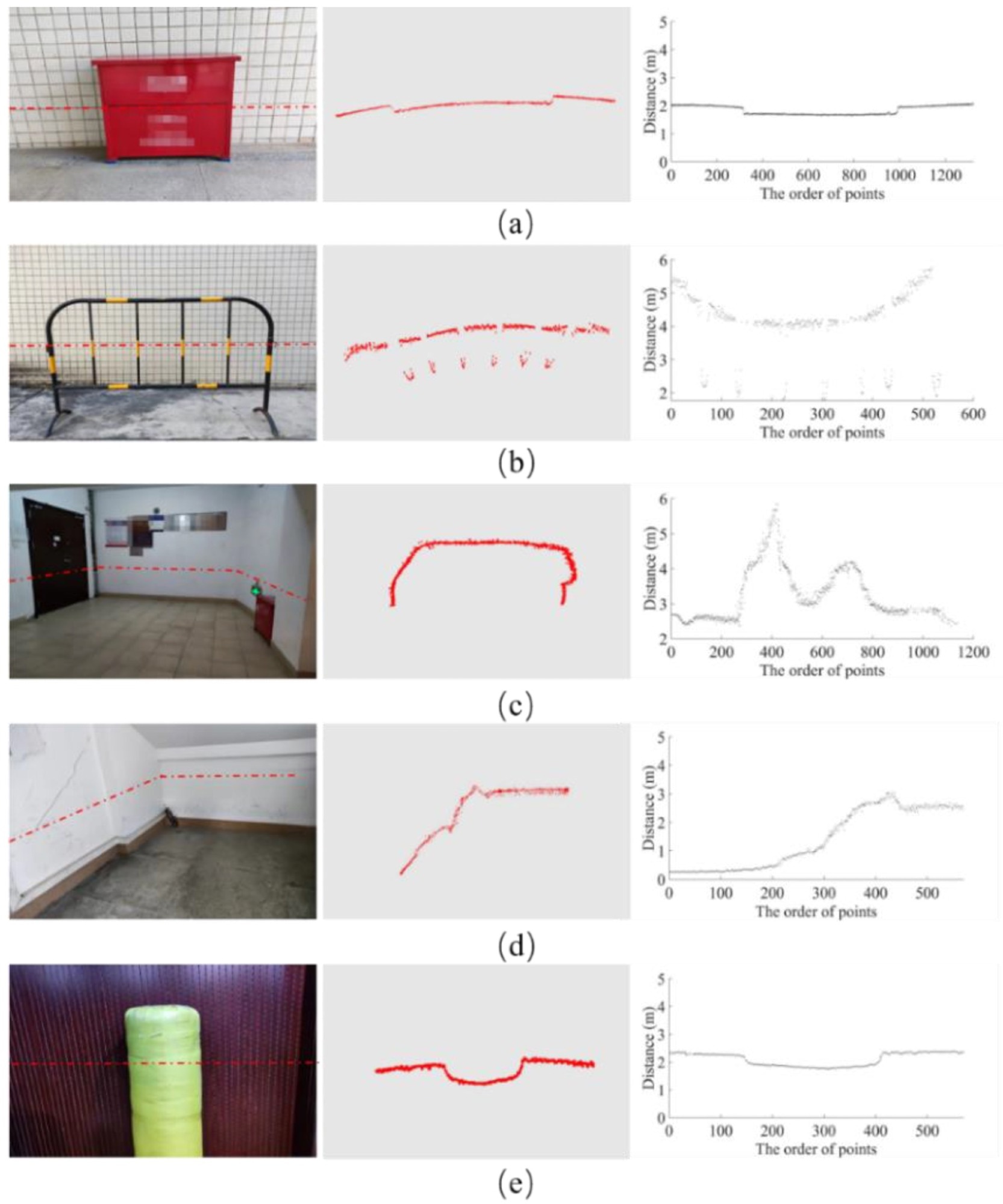
Figure 13. Scanning results. (a) Continuous object scanning; (b) Discontinuous object scanning; (c) Wide-view scanning; (d) Rectangular object scanning; (e) Circular object scanning. Image Credit: Huang, et al., 2022
Conclusion
In conclusion, a digitally transformed 2D LiDAR system with a lightweight and resource-saving TDC based on a symmetrical tapped delay line is incorporated in a low-end FPGA. To measure distance, the LiDAR utilizes the ToF ranging technique. It is made up of a homemade transceiver and a mechanical scanning structure made from off-the-shelf components.
This structure eliminates the expense and dimensions of LiDAR, which is important in consuming applications. Furthermore, due to its low cost and high integration, the presented digitally integrated LiDAR could be used in smart cities for robotic navigation, real-time pedestrian counting, truck overload tracking, social distance recognition, and traffic surveillance applications.
Journal Reference:
Huang, J., Ran, S., Wei, W., Yu, Q. (2022) Digital Integration of LiDAR System Implemented in a Low-Cost FPGA. Symmetry, 14(6), p. 1256. Available Online: https://www.mdpi.com/2073-8994/14/6/1256/htm.
References and Further Reading
- Xu, P., et al. (2020) Design and validation of a shipborne multiple-field-of-view lidar for upper ocean remote sensing. Journal of Quantitative Spectroscopy and Radiative Transfer, 254, p. 107201. doi.org/10.1016/j.jqsrt.2020.107201.
- Li, M., et al. (2020) Modeling and analyzing point cloud generation in missile-borne LiDAR. Defence Technology, 16, pp. 69–76. doi.org/10.1016/j.dt.2019.10.003.
- Wang, L., et al. (2017) Map-based localization method for autonomous vehicles using 3D-LIDAR. IFAC-PapersOnLine, 50, pp. 276–281. doi.org/10.1016/j.ifacol.2017.08.046.
- Onda, K., et al. (2018) Dynamic environment recognition for autonomous navigation with wide FOV 3D-LiDAR. IFAC-PapersOnLine, 51, pp. 530–535. doi.org/10.1016/j.ifacol.2018.11.579.
- Javanmardi, E., et al. (2017) Autonomous vehicle self-localization based on probabilistic planar surface map and multi-channel LiDAR in urban area. In Proceedings of the 2017 IEEE 20th International Conference on Intelligent Transportation Systems (ITSC), Yokohama, Japan, 16–19 October.
- Behroozpour, B., et al. (2017) Lidar system architectures and circuits. IEEE Communications Magazine, 55, pp. 135–142. https://doi.org/10.1109/MCOM.2017.1700030.
- Malka, V., et al. (2008) Principle and applications of electron beams produced with laser plasma accelerators. Journal of Physics Conference Series, 112, p. 042029. doi.org/10.1088/1742-6596/112/4/042029.
- Chen, X., et al. (2020) High-repetition-rate, sub-nanosecond and narrow-bandwidth fiber-laser-pumped green laser for photon-counting shallow-water bathymetric Lidar. Results in Physics, 19, p. 103563. doi.org/10.1016/j.rinp.2020.103563.
- Wu, D., et al. (2022) Multi-beam single-photon LiDAR with hybrid multiplexing in wavelength and time. Optics & Laser Technology, 145, p. 107477. doi.org/10.1016/j.optlastec.2021.107477.
- Chen, Z., et al. (2018) Accuracy improvement of imaging lidar based on time-correlated single-photon counting using three laser beams. Optics Communications, 429, pp. 175–179. doi.org/10.1016/j.optcom.2018.08.017.
- Palani, L., et al. (2020) Area efficient high-performance time to digital converters. Microprocessors and Microsystems, 73, p. 102974. doi.org/10.1016/j.micpro.2019.102974.
- Christiansen, J (2012) Picosecond stopwatches: The evolution of time-to-digital converters. IEEE Solid-State Circuits Magazine, 4, pp. 55–59. doi.org/10.1109/MSSC.2012.2203189.
- Gagnon, H., et al. (2010) TARGETED MASS spectrometry imaging: Specific targeting mass spectrometry imaging technologies from history to perspective. Progress in Histochemistry and Cytochemistry, 47, pp. 133–174. doi.org/10.1016/j.proghi.2012.08.002.
- Maatta, K & Kostamovaara, J (1998) A high-precision time-to-digital converter for pulsed time-of-flight laser radar applications. IEEE Transactions on Instrument Measurement, 47, pp. 521–536. doi.org/10.1109/19.744201.
- Caram, J.P., et al. (2015) Harmonic ring oscillator time-to-digital converter. In Proceedings of the 2015 IEEE International Symposium on Circuits and Systems (ISCAS), Lisbon, Portugal, 24–27 May; pp. 161–164.
- Tontini, A., et al. (2018) Design and characterization of a low-cost FPGA-based TDC. IEEE Transaction on Nuclear Science, 65, pp. 680–690. doi.org/10.1109/TNS.2018.2790703.
- Sui, T., et al. (2019) A 2.3-ps RMS resolution time-to-digital converter implemented in a low-cost cyclone V FPGA. IEEE Transactions Instrument Measurement, 68, pp. 3647–3660. doi.org/10.1109/TIM.2018.2880940.
- Nogrette, F., et al. (2015) Characterization of a detector chain using a FPGA-based time-to-digital converter to reconstruct the three-dimensional coordinates of single particles at high flux. Review of Scientific Instruments, 86, p. 113105. doi.org/10.1063/1.4935474.
- Song, J., et al. (2006) A high-resolution time-to-digital converter implemented in field-programmable-gate-arrays. IEEE Transaction on Nuclear Science, 53, pp. 236–241. doi.org/10.1109/TNS.2006.869820.
- Zhao, L., et al. (2013) The design of a 16-channel 15 ps TDC implemented in a 65 nm FPGA. IEEE Transaction on Nuclear Science, 60, pp. 3532–3536. doi.org/10.1109/TNS.2013.2280909.
- Kwiatkowski, P & Szplet, R (2020) Efficient implementation of multiple time coding lines-based TDC in an FPGA device. IEEE Transanction on Instrument Measurement, 69, pp. 7353–7364. doi.org/10.1109/TIM.2020.2984929.
- Dadouche, F., et al. (2015) New design-methodology of high-performance TDC on a low cost FPGA targets. Sensors & Transducers, 193, pp. 123–134.
- Wang, J., et al. (2020) A fully fledged TDC implemented in field-programmable gate arrays. IEEE Transactions on Nuclear Science, 57, pp. 446–450. doi.org/10.1109/TNS.2009.2037958.
- Lusardi, N., et al. (2019) Digital instrument with configurable hardware and firmware for multi-channel time measures. Review of Scientific Instruments, 90, p. 055113. doi.org/10.1063/1.5028131.
- Xia. X., et al. (2019) A novel TDC/ADC hybrid reconstruction ROIC for LiDAR. IEICE Electronics Express, 16, p. 20181076. doi.org/10.1587/elex.16.20181076.
- Seo, H., et al. (2020) A 36-Channel SPAD-Integrated Scanning LiDAR Sensor with Multi-Event Histogramming TDC and Embedded Interference Filter. In Proceedings of the 2020 IEEE Symposium on VLSI Circuits, Honolulu, HI, USA, 16–19 June 2020.
- Lesani, A., et al. (2020) Development and evaluation of a real-time pedestrian counting system for high-volume conditions based on 2D LiDAR. Transportation Research Part C: Emerging Technologies, 114. pp. 20–35. doi.org/10.1016/j.trc.2020.01.018.
- Tai, T.S., et al. (2022) 3D LIDAR based on FPCB mirror. Mechatronics, 82, p. 102720. doi.org/10.1016/j.mechatronics.2021.102720.
- Seferiadis, G., et al. (2006) FPGA implementation of a delay-line readout system for a particle detector. Measurement, 39, pp. 90–99. doi.org/10.1016/j.measurement.2005.07.003.
- Machado, R., et al. (2019) Recent developments and challenges in FPGA-based time-to-digital converters. IEEE Transactions on Instrument Measurement, 68, pp. 4205–4221. doi.org/10.1109/TIM.2019.2938436.
- Machado, R., et al. (2019) Recent developments and challenges in FPGA-based time-to-digital converters. IEEE Transactions on Instrument Measurement, 68, pp. 4205–4221. https://doi.org/10.1109/TIM.2019.2938436.
- Maamoun, M., et al. (2017) A 3 ps resolution time-to-digital converter in low-cost FPGA for laser rangefinder. Proceedings of the World Congress on Engineering, 1, pp. 7–11.
- Chen, P., et al. (2016) A high resolution FPGA TDC converter with 2.5 ps bin size and -3.79~6.53 LSB integral nonlinearity. In Proceedings of the 2016 2nd International Conference on Intelligent Green Building and Smart Grid (IGBSG), Prague, Czech Republic, 27–29 June 2016.
- Prasad, K., et al. (2022) An FPGA based 33-channel, 72 ps LSB time-to-digital converter. Nuclear Instruments and Methods in Physics Research Section A: Accelerators, Spectrometers, Detectors and Associated Equipment, 1027, p. 166052. doi.org/10.1016/j.nima.2021.166052.
- OSRAM Opto Semiconductors, SPL PL90_3_EN Datasheet, Radial T1 ¾ (2018). Available at: https://dammedia.osram.info/media/resource/hires/osram-dam-6189135/SPL%20PL90_EN.pdf
- First Sensor APD Data Sheet, Part Description AD500-9 SMD, Order # 501122; 501818, Version 20-06-11. Available at: https://www.first-sensor.com/cms/upload/datasheets/AD500-9_SMD_3001495.pdf