Materials patterning and sorting are critical for a wide range of materials applications. The current materials technologies such as additive manufacturing and microfluidics have made them possible. In recent years, additive manufacturing, commonly known as 3D printing, has gained a lot of interest as a powerful fabrication process for complex structures.

Image Credit: FrameStockFootages/Shutterstock.com
Fused deposition modeling, stereolithography, and selective laser sintering are some of the common processes used in 3D printing. Such technologies, on the other hand, have the drawback of only using a single supply of material in the nozzle during the printing process.
Dielectrophoresis (DEP) is a material sorting process that involves applying a force to a dielectric material in a non-uniform electric field present in a liquid medium. Many DEP research is conducted in aqueous settings, making it difficult to adapt directly to printing technology’s ambient conditions.
Researchers have demonstrated multi-material patterning and materials sorting through a single nozzle in ambient conditions using a DEP-empowered Pipette/QTF-AFM (DEPQA). The results offer a new perspective on multi-material patterning and materials sorting, as well as a broader perspective on additive manufacturing, and increasing the applicability of DEP-based research and industry.
Methodology
The DEPQA system is seen schematically in Figure 1.
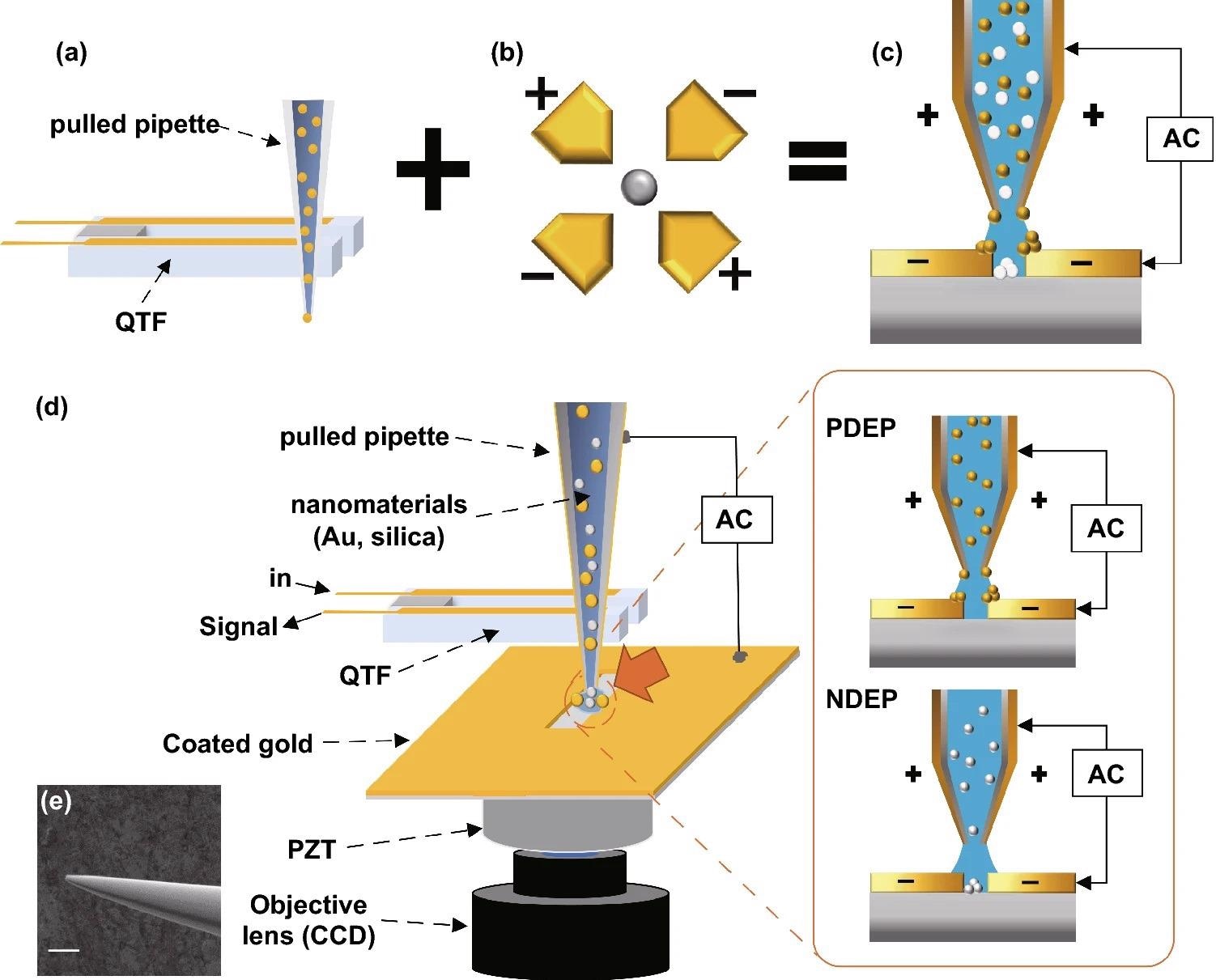
Figure 1. Schematic diagram of the experiment. (a) QTF-AFM with a pulled pipette system. It has strength in efficient low-volume liquid delivery. (b) Quadrupole DEP trap. If the Clausius–Mossotti factor is below zero, solutes receive a negative-DEP force and go to the center of the electrodes. (c)We propose the DEP-based material-selective deposition technique using the pipette-AFM system. The pipette-AFM delivers the low-volume solution to the desired position and DEP forces deposited nanoparticles on the edge or middle position of electrodes. Yellow particles show the positive-DEP effect and white particles show the negative-DEP effect. (d) Detailed schematic diagram of the experimental setup. XY positioning of the pipette on the scratched gap is enacted while watching the optical microscope image of CCD in real-time, and the Z positioning (approach and retract) of the pipette is enacted under QTF-AFM feedback. An AC voltage is applied between the coated Au layer on the glass substrate and the surfaces of the Au-coated pulled pipette. (e) Detailed SEM image of the coated pulled pipette, 10 µm scale bar. Image Credit: Kim, et al., 2022
Results
Figure 2 depicts the pre-examination simulation results used to determine the experimental parameter. The frequency and real component of fCM of a 100 nm diameter silica nanoparticle are calculated in Figure 2(a). In the experimental scheme with the directions in Figure 2(b), Figure 2(c, d) shows the trapped energy from the PDEP force vs. the Brownian motion energy (= kBT).
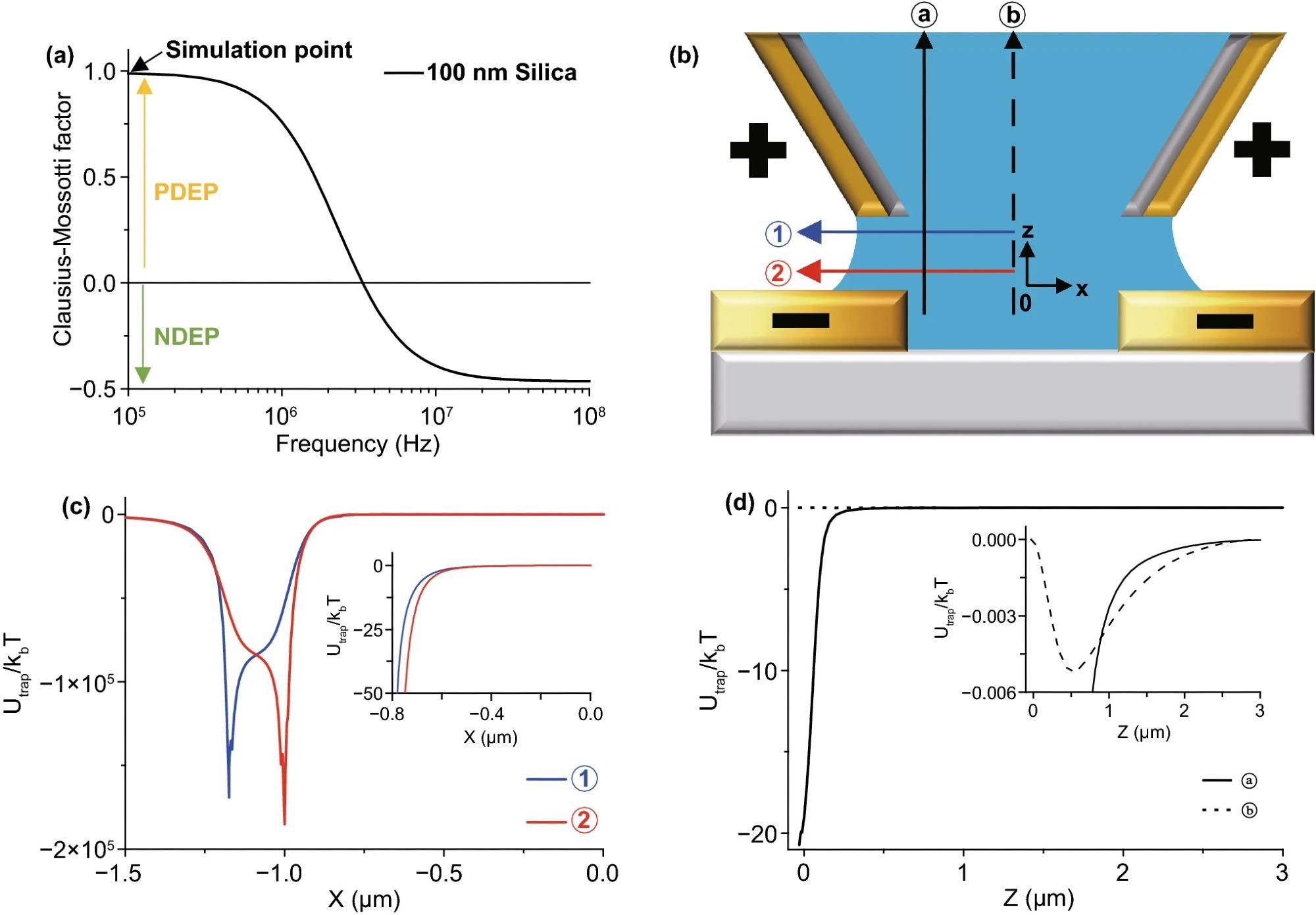
Figure 2. (a) An example graph of Clausius–Mossotti factor (fCM) of 100 nm diameter silica nanoparticles. The sign of fCM determines PDEP or NDEP. The critical frequency of the sign is almost 3 MHz in this case. (b) Schematic diagram of the experiment with arrows for the X- and Z-directions. The phase of electrodes is determined by the simulation in Fig. S1. (c) Simulation graph of PDEP (fCM = 1.0) trap energy vs. Brownian motion along the X-axis. Vpeak = 1.0 V, 15 MHz frequency of AC voltage, 100 nm diameter of the particle, 2.0 µm gap size, and 2.35 µm outer diameter of the pipette with a 0.7 Rinner/Router ratio. The trap energy rapidly increases around the edge of electrodes near the outer diameter of the pipette at ① (±1.175 µm) and substrate at ② (±1.0 µm), so the particles affected by the PDEP force are supposed to move to the edge of the electrodes. The inset image shows an expanded graph near the center; it shows the same direction for the PDEP force. The NDEP case shown in Fig. S3 and the particles affected by NDEP gather around the center near zero. (d) Simulation graph of the DEP trap energy vs. Brownian motion along the Z-axis with the same conditions as (c). The particles affected by PDEP force are supposed to move downward at ⓐ but the particles affected by NDEP go upward. However, in the inset graph, the Brownian motion energy is much bigger than the z-direction DEP trap energy at ⓑ, so particles are not affected by the DEP force in the Z-direction except near ⓐ. Image Credit: Kim, et al., 2022
By measuring the amplitude signal of the QTF sensor during liquid supply and materials deposition, researchers discovered two distinct particle behaviors. Predicting expected signal outcomes for metallic and dielectric particles can help determine if the solute, solvent, and surfactants employed in the solution are appropriate for achieving non-aggregation roles before receiving the FESEM picture of the results.
The simulation result of the frequency and actual part of the fCM of the nanoparticles utilized in the tests is shown in Figure 3(a). SEM photographs of the experimental results are shown in Figure 3(b–e). In Figure 3(b), Au nanoparticles are deposited in a circular form, which can be observed as an attraction to the substrate’s electrode edges and the pipette’s round apex; PDEP. In Figure 3(c), the tendency of silica nanoparticles is comparable to that of Au, which may also be seen as PDEP. A mixed solution's selectively deposited outcome is shown in Figure 3(e).
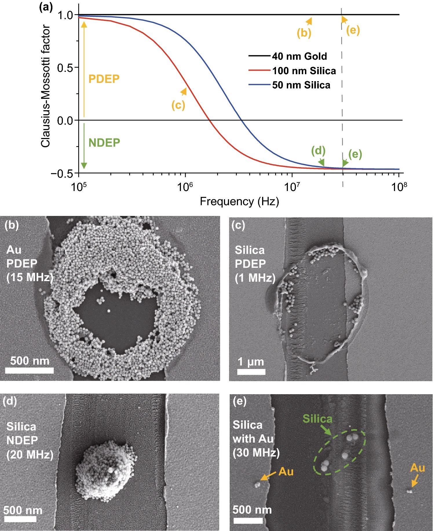
Figure 3. SEM images of PDEP and NDEP experiments. (a) Clausius–Mossotti factor (fCM) of nanoparticles used for experiments. Several characteristics (εm/p, σm/p, σbulk, Ks) of Au and silica nanoparticles are from reference. The X-axis is a log scale of the frequency (Hz). Signs of fCM change at ~2 MHz (100 nm silica), ~4 MHz (50 nm silica), and fCM of 40 nm Au always has a plus sign in the 0.1–100 MHz range. Arrows show the frequencies used, and colors indicate PDEP (yellow) or NDEP (green). (b) PDEP result of Au nanoparticles with 40 nm diameter Au nanoparticles, ~2 µm diameter pipette with Rinner/Router ratio = 0.7, Vpeak= 1.0 V, and 15 MHz frequency. Particles are attracted to surface electrodes of the substrate and the pipette. (c) PDEP result of silica nanoparticles with 100 nm diameter silica nanoparticles, ~ 2 µm diameter pipette, Vpeak= 2.5 V and 1 MHz frequency. Particles show the same tendency as in (a). The concentration and surfactants of nanoparticle solutions result in differences between (b) and (c). (d) NDEP result of silica nanoparticles with 50 nm diameter silica nanoparticles, ~1.5 µm diameter pipette, Vpeak= 2.5 V, and 20 MHz frequency. Particles move off to the surface electrodes of the substrate and pipette and gather around the center of the pipette. (e) Sorting result of the mixed solution with 100 nm diameter silica nanoparticles and 20 nm diameter Au nanoparticles, Vpeak= 2.5 V, and 30 MHz frequency. Silica nanoparticles in the green circle show NDEP and Au nanoparticles next to the yellow arrows show PDEP. Image Credit: Kim, et al., 2022
Beyond the proof-of-principle demonstration of the sorting function described, a more extended and detailed search for the optimal appropriate surfactants and solutions for the mixed scenario will undoubtedly improve the sorting function.
In other words, the Electrothermal effect (ETE) is the primary cause of decreased spatial deposition accuracy at higher voltages, and it is critical to utilize the optimal AC voltage value that produces sufficient DEP force and a low rate of ⟨FETE⟩/⟨FDEP⟩.
Discussion
Figure 4 illustrates the selective deposition’s SERS effect application. The 4-nitrobenzenethiol Raman signal (Figure. 4b) was found primarily in the deposited region of Au nanoparticles (Figure. 4a). Furthermore, the Raman intensity vs. particle number is linearly well fitted in Figure. 4c, indicating that the Au nanoparticles in the data display the SERS effect.
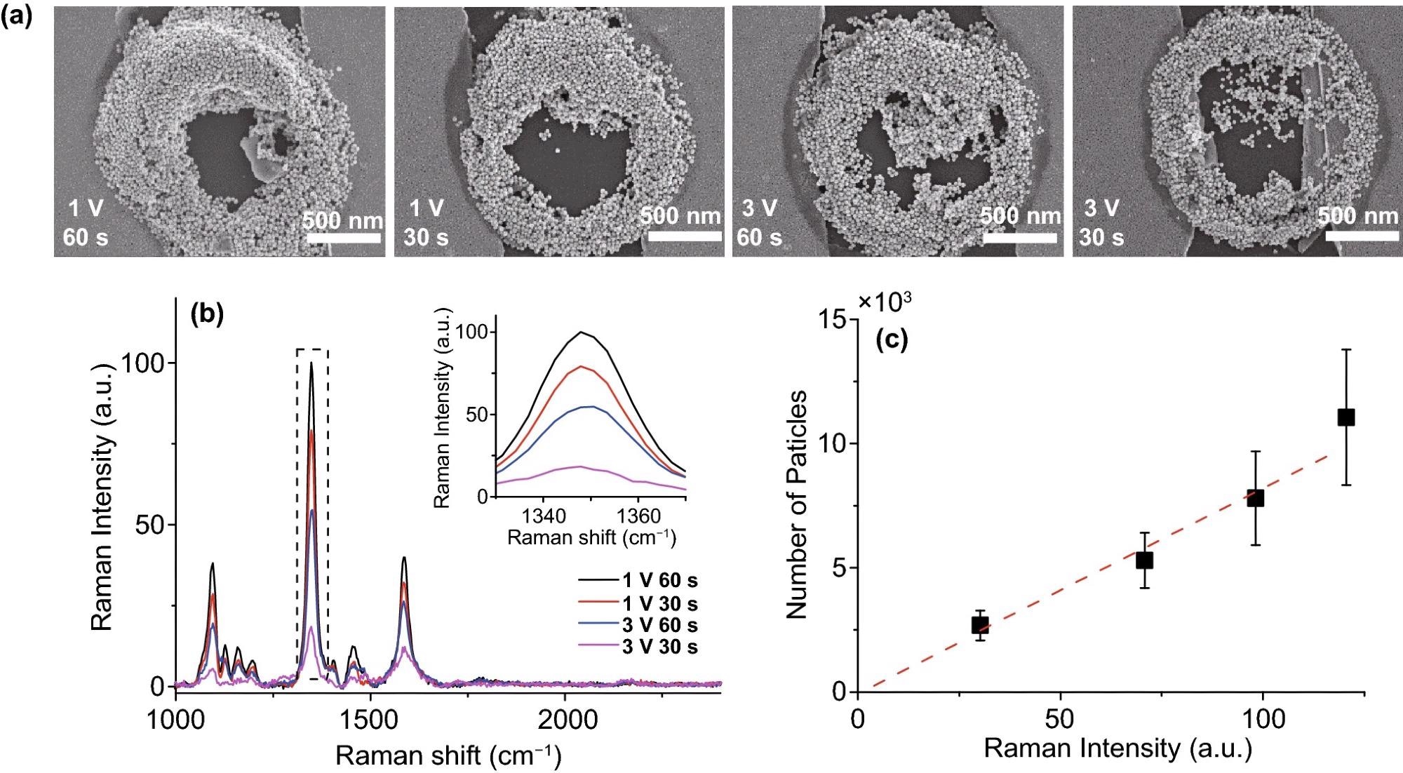
Figure 4. SERS results of various PDEP Au nano-aggregates samples. (a) SEM images of Au nano-aggregates deposited by PDEP; 500 nm scale bar. (b) SERS spectra of various Au nano-aggregates coated with 4-nitrobenzenethiol; the inset graph is the expanded spectra in the dotted line (nitro group). (c) Raman intensity and particle count graph. The ratio of Raman intensity of peaks in the inset graph of (b) is linearly well-fitted (red dashed line) with the ratio of the number of Au nanoparticles, which indicates that Au nanoparticles enhanced Raman signal. Therefore, the system can be used for the fabrication of the nano-micro-SERS platform by the enrichment of nanoparticles such as in the coffee-ring effect. Image Credit: Kim, et al., 2022
Conclusion
Selective deposition of several materials in a single nozzle can give a wide range of additive manufacturing capabilities, allowing for a wider variety of materials and streamlined procedures. The DEP effect was seen in Au nanoparticles and silica nanoparticles, as predicted by the modeling, and they were preferentially deposited spatially at the predicted frequency. The electrothermal effect, which might be a problem for this system, was investigated, and the proper voltage range was discovered.
In addition, scientists confirmed that they could roughly monitor particle dynamics using QTF signals and that this experimental finding had a SERS impact. With the help of a single pipette and the DEP of Au and silica nanoparticles, researchers were able to prove the viability of selective deposition utilizing the DEP of Au and silica nanoparticles.
Researchers proved the possibility of selective deposition utilizing DEP of Au and silica nanoparticles using a single pipette in ambient settings with simulated parameters using QTF-AFM guidance. In addition, the SERS effect was validated by monitoring the dynamics of nanoparticles contained in a water channel in real-time.
However, by making the system more user-friendly, DEPQA could become a robust tool for nanoscale sorting and fabricating three-dimensional structures in ambient conditions, such as 3D nanowires with metal-bound and dielectric cores or other complex structures, which could be useful for 3D printing’s additive manufacturing feature.
In addition, the demonstration has the potential to further enhance DEP's capabilities, which may be used in SERS, nano-micro selective patterning, materials sorting, biomedical engineering, and a variety of other applications.
Journal Reference:
Kim, C., Hong, S., Shin, D., An, S., Zhang, X., Jhe, W. (2022) Sorting Gold and Sand (Silica) Using Atomic Force Microscope-Based Dielectrophoresis. Nano-Micro Letters, 14(1), pp.1–11. Available Online: https://link.springer.com/article/10.1007/s40820-021-00760-x.
References and Further Reading
- Delawder, A O & Barnes, J C (2020) Precise patterning driven by droplets. Nature Chemistry, 12, pp. 328–330. doi.org/10.1038/s41557-020-0449-9.
- Zhang, R., et al. (2021) Spatiotemporal control of liquid crystal structure and dynamics through activity patterning. Nature Materials, 20, pp. 875–882. doi.org/10.1038/s41563-020-00901-4.
- Wang, S., et al. (2021) Machine-learning micropattern manufacturing. Nano Today, 38, p. 101152. doi.org/10.1016/j.nantod.2021.101152.
- Nawaz, A. A., et al. (2020) Intelligent image-based deformation-assisted cell sorting with molecular specificity. Nature Methods, 17, pp. 595–599. https://doi.org/10.1038/s41592-020-0831-y.
- Chowdhury, M. S., et al. (2021) Functional surfactants for molecular fishing, capsule creation, and single-cell gene expression. Nano-Micro Letters, 13, p. 147. https://doi.org/10.1007/s40820-021-00663-x.
- Chowdhury, M. S., et al. (2019) Dendronized fluorosurfactant for highly stable water-in-fluorinated oil emulsions with minimal inter-droplet transfer of small molecules. Nature Communications, 10, p. 4546. doi.org/10.1038/s41467-019-12462-5.
- Wang, Y., et al. (2020) Microenvironment-controlled micropatterned microfluidic model for biomimetic in-situ studies. ACS Nano, 14, pp. 9861–9872. doi.org/10.1021/acsnano.0c02701.
- Fujiwara, H., et al. (2021) Optical selection and sorting of nanoparticles according to quantum mechanical properties. Science Advances, 7(3), p. eabd9551. doi.org/10.1126/sciadv.abd9551.
- Liu, L., et al. (2020) Step emulsification: high throughput production of monodisperse droplets. BioTechniques, 68, pp. 114–116. doi.org/10.2144/btn-2019-0134.
- Jung, W., et al. (2021) Three-dimensional nanoprinting via charged aerosol jets. Nature, 592, pp. 54–59. doi.org/10.1038/s41586-021-03353-1.
- Loke, G., et al. (2019) Structured multimaterial filaments for 3D printing of optoelectronics. Nature Communications, 10, p. 4010. doi.org/10.1038/s41467-019-11986-0.
- Yuk, H., et al. (2020) 3D printing of conducting polymers. Nature Communications, 11, p. 1604. doi.org/10.1038/s41467-020-15316-7.
- Daminabo, S. C., et al. (2020) Fused deposition modeling-based additive manufacturing (3D printing): techniques for polymer material systems. Materials Today Chemistry, 16, p. 100248. https://doi.org/10.1016/j.mtchem.2020.100248.
- Yin, H., et al. (2018) Orthogonal programming of heterogeneous micro-mechano-environments and geometries in three-dimensional bio-stereolithography. Nature Communications, 9, p. 4096. doi.org/10.1038/s41467-018-06685-1.
- Helmer, D., et al. (2020) Divide and print. Nature Materials, 19, pp. 131–133. doi.org/10.1038/s41563-019-0594-y.
- Eisenstein, M., et al. (2006) Divide and conquer. Nature, 441, pp. 1179–1185. https://doi.org/10.1038/4411179a.
- Wang, X., et al. (2020) Positive dielectrophoresis–based Raman-activated droplet sorting for culture-free and label-free screening of enzyme function in vivo. Science Advances, 6(32), p. eabb3521. doi.org/10.1126/sciadv.abb3521.
- Wang, Q., et al. (2019) Microfluidic dielectrophoresis illuminates the relationship between microbial cell envelope polarizability and electrochemical activity. Science Advances, 5(1), p. eaat5664. doi.org/10.1126/sciadv.aat5664.
- Gérard, A., et al. (2020) High-throughput single-cell activity-based screening and sequencing of antibodies using droplet microfluidics. Nature Biotechnology, 38, pp. 715–721. doi.org/10.1038/s41587-020-0466-7.
- Isozaki, A., et al. (2020) Sequentially addressable dielectrophoretic array for high-throughput sorting of large-volume biological compartments. Science Advances, 6(22), p. 6712. doi.org/10.1126/sciadv.aba6712.
- Yu, E. S., et al. (2020) Precise capture and dynamic relocation of nanoparticulate biomolecules through dielectrophoretic enhancement by vertical nanogap architectures. Nature Communications, 11, p. 2804. doi.org/10.1038/s41467-020-16630-w.
- Krupke, R., et al. (2003) Separation of metallic from semiconducting single-walled carbon nanotubes. Science, 301(5631), pp. 344–347. doi.org/10.1126/science.1086534.
- Tang, L., et al. (2021) Combined quantum tunnelling and dielectrophoretic trapping for molecular analysis at ultra-low analyte concentrations. Nature Communications, 12, p. 913. doi.org/10.1038/s41467-021-21101-x.
- An, S., et al. (2012) Low-volume liquid delivery and nanolithography using a nanopipette combined with a quartz tuning fork-atomic force microscope. Nanoscale, 4, pp. 6493–6500. doi.org/10.1039/C2NR30972F.
- Lee, M., et al. (2016) Viscometry of single nanoliter-volume droplets using dynamic force spectroscopy. Physical Chemistry Chemical Physics, 18, pp. 27684–27690. doi.org/10.1039/C6CP05896E.
- Kim, S., et al. (2018) Direct evidence for curvature-dependent surface tension in capillary condensation: Kelvin equation at molecular scale. Physical Review X, 8, p. 041046. doi.org/10.1103/PhysRevX.8.041046.
- An, S., et al. (2019) Buckling tip-based nanoscratching with in situ direct measurement of shear dynamics. Applied Nanoscience. 9, pp. 67–76. doi.org/10.1007/s13204-018-0897-3.
- Oh, J., et al. (2009) Comprehensive analysis of particle motion under non-uniform AC electric fields in a microchannel. Lab Chip, 9, pp. 62–78. doi.org/10.1039/B801594E.
- Honegger, T., et al. (2011) Determination of Clausius-Mossotti factors and surface capacitances for colloidal particles. Applied Physics Letters, 98, p. 181906. doi.org/10.1063/1.3583441.
- An, S., et al. (2013) Compensation of stray capacitance of the quartz tuning fork for a quantitative force spectroscopy. Current Applied Physics, 13, pp. 1899–1905. doi.org/10.1016/j.cap.2013.07.024.
- Castellanos-Gomez, A., et al. (2009) Dynamics of quartz tuning fork force sensors used in scanning probe microscopy. Nanotechnology, 20, p. 215502. doi.org/10.1088/0957-4484/20/21/215502.
- Kim, J., et al. (2014) Effective stiffness of qPlus sensor and quartz tuning fork. Ultramicroscopy, 141, pp. 56–62. doi.org/10.1016/j.ultramic.2014.03.009.
- Morgan, H & Green, N G (2003) Electrokinetics. Colloids and Nanoparticles (Research Studies Press, Philadelphia, PA), pp.152–159.
- Ramos, A., et al. (1998) AC electrokinetics: a review of forces in microelectrode structures. Journal of Physics D. Applied Physics, 31, pp. 2338–2353. doi.org/10.1088/0022-3727/31/18/021.
- Wang, W., et al. (2014) Coffee-ring effect-based simultaneous SERS substrate fabrication and analyte enrichment for trace analysis. Nanoscale, 6, pp. 9588–9593. doi.org/10.1039/C4NR03198A.
- Shin, D., et al. (2019) Ice-VII-like molecular structure of ambient water nanomeniscus. Nature Communications, 10, p. 286. doi.org/10.1038/s41467-019-08292-0.