Plasmonics has opened a route to sub-diffraction limit control of light and is a way of trying to miniaturize optical devices. Plasmonic interactions usually involve surface plasmon polaritons – coherent oscillations of the electrons on the surface of a dielectric material. By tuning the design of the device to control these oscillations, it is possible to channel visible light on the nanometer scale.
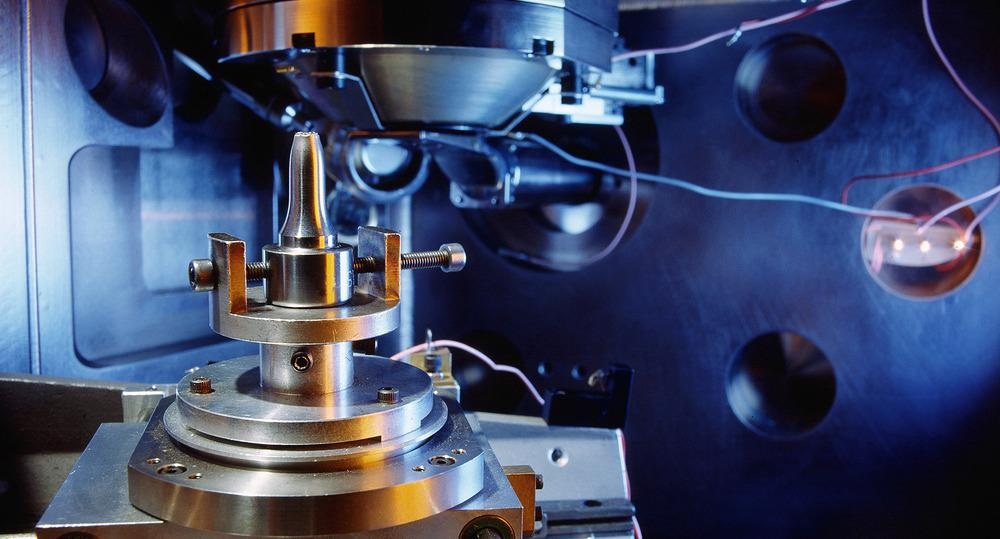
Image Credit: Bildagentur Zoonar GmbH/Shutterstock.com
While plasmonic effects have been exploited in many applications, including signal enhancements in Raman spectroscopy and for molecular recognition and sensing,1 there are many unanswered questions as to the exact details of the mechanisms involved in these plasmonic enhancements. This is further complicated as there is a spatial component to the plasmonic effects and interactions, which requires imaging techniques to probe.
Gold and silver nanoparticles and structures have become commonplace in nanoplasmonic devices. The widespread use of gold and silver is because they are highly stable metals, readily form nanostructures in a controllable way, and can support plasmonic modes across most of the visible to near infra-red region owing to the dielectric function of the materials.2
To create functional devices for sensing, there has been a great deal of interest in combining metal nanostructures with materials suitable for use in optoelectronics. These so-called hybrid plasmonic systems can have interactions between the more traditional metal center and the material due to couplings that arise when the two species are at short distances.
Using Ultrafast Electron Microscopy to Investigate Nanoparticles and Graphene
A team based at the U.S. Department of Energy's (DOE) Argonne National Laboratory has been using ultrafast electron microscopy to investigate these strong couplings that arise between gold nanoparticles and layers of the two-dimensional material, graphene.3 The team’s research was published in the journal Nano Letters.
Graphene is a form of carbon that is only one layer thick with highly unusual properties, including excellent electrical conductivity. By combining graphene and its outstanding charge-carrying capabilities with the light-conducting powers of plasmonic nanostructures, it is possible to envision new architectures for high-performance optoelectronic devices.
Ultrafast Electron Microscopy
The team at Argonne National Laboratory was able to use high-resolution microscopy with electrons to visualize exactly what was happening in the region between the gold nanostructure and the graphene. This is where they noticed some unusual behavior in the graphene because of the coupling between the two systems.
Depending on the relative position of the gold nanoparticle to the graphene surface, the distribution and the shape of the plasmonic fields were changed. With the nanoparticle sitting flat on the graphene sheet, the plasmonic fields remained symmetric. However, if the nanoparticle was moved to the edge of the graphene sheet, there was a localization of plasmonic fields in the edge region.
To investigate this phenomenon, the team used a technique called ultrafast electron microscopy. Electron microscopes are often used for their very high spatial resolution to capture images on the nanometer scale. With advances in the generation of ultrashort electron pulses and the availability of ultrafast laser pulses, it is now possible to combine both types of pulse in a single experiment.
In these experiments on graphene and gold nanoparticles, the team used a short laser pulse to interact with the sample and trigger a response from the electrons, and then an ultrafast electron bunch to collect electron microscope images with excellent time resolution. The advantage of ultrafast techniques such as ultrafast electron microscopy is that they have time resolutions sufficiently short to capture the processes that unfold in materials after they have interacted with light. Many of these occur on a femtosecond timescale and so are too quick to be captured with more conventional microscopy techniques.
The spatial resolution of the electron microscopy and the time resolution of the setup made it possible to visualize the evolution of the plasmonic fields following the photoexcitation event and how this hybrid system could be used to manipulate light on the nanoscale.
Plasmonic Fundamentals
Given the importance of ultrafast processes in light-matter interactions and the formation of transient non-equilibrium states, access to tools such as ultrafast electron microscopy will allow us to directly capture information on these states and processes and design new generations of plasmonic materials to manipulate these properties. At present, there is still very little known about the coupling mechanisms in hybrid plasmonic systems and fewer attempts still to watch them in the act of energy transfer for plasmonic field manipulation.
The team at Argonne National Laboratory will be opening its capabilities to the wider user community to see how this ability to probe new types of information can revolutionize our development of sensors and quantum devices.
References and Further Reading
- Boken, J., Khurana, P., Thatai, S., Kumar, D., & Prasad, S. (2017). Plasmonic nanoparticles and their analytical applications: A review. Applied Spectroscopy Reviews, 52(9), 774–820. https://doi.org/10.1080/05704928.2017.1312427
- Liz-Marzán, L. M., Murphy, C. J., & Wang, J. (2014). Nanoplasmonics. Chemical Society Reviews, 43(11), 3820–3822. https://doi.org/10.1039/c4cs90026j
- Liu, H., Gage, T. E., Singh, P., Jaiswal, A., Schaller, R. D., Tang, J., Park, S. T., Gray, S. K., & Arslan, I. (2021). Visualization of Plasmonic Couplings Using Ultrafast Electron Microscopy. Nano Letters, 21(13), 5842–5849. https://doi.org/10.1021/acs.nanolett.1c01824
Disclaimer: The views expressed here are those of the author expressed in their private capacity and do not necessarily represent the views of AZoM.com Limited T/A AZoNetwork the owner and operator of this website. This disclaimer forms part of the Terms and conditions of use of this website.