Updated on 17 August 2021.
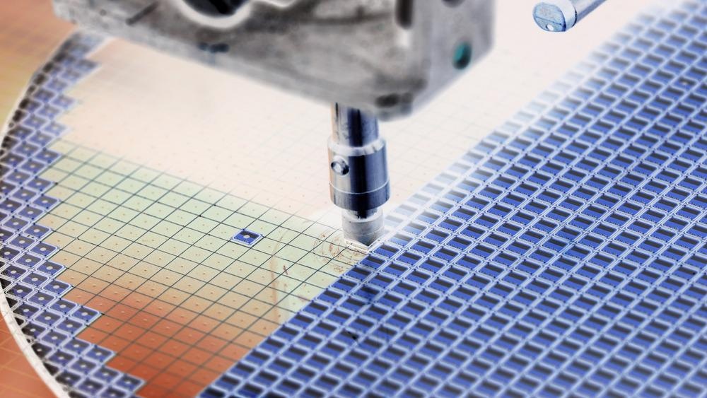
Image Credit: Macro photo/Shutterstock.com
Dimensional scaling of materials is essential in many industries. To overcome its limitations, new engineering methods and techniques need to be used. One such technique is scanning microwave impedance microscopy (sMIM), which can be used to obtain information about the electrical properties of a material as well as its metrology.
In device characterization research, the physical properties of a material are often studied by investigating the response from electromagnetic excitations. With the growth of the number of compounds used in electronic devices, new methods must be introduced to keep up with the demand of different industries, such as the semiconductor industry.
What is sMIM?
SMIM is a near-field technique that uses a combination of a microwave source and atomic force microscopy (AFM). In this technique, the cantilever tip of an AFM is used as a source of microwaves to obtain information about the electrical properties of materials. This setup can be used to investigate the properties of a material such as resistivity, permittivity, dielectric constant, dopant concentration, and capacitance.
The reflected signal carries information about the permittivity and conductivity variations in the sample, which can be used to obtain the resistivity and capacitance. Obtaining information about the capacitance of a sample is essential since it can be used to determine the dopant concentration in semiconductors.
Similarly to AFM, sMIM has different modes such as tapping, contact, and non-contact mode. It works by delivering a microwave signal to the tip of an AFM cantilever and can scan through the sample to collect the reflected signal. The nanotip used has two functions: it delivers the microwave signal and receives the reflected signal.
sMIM is a non-invasive technique with resolution beyond the diffraction limit. However, unlike AFM, sMIM can be used to obtain information about the microwave impedance of a material that does not depend on surface properties, as well as measurements below the surface due to the penetration abilities of microwaves.
The Lifetime of the sMIM Tip
When working with a sharp tip, such as the one used in sMIM, it is important to consider the lifetime of the probe and the tip wear which affects the contrast in the measurements. The number of times a probe can be used before it is destroyed depends largely on the type of surfaces that are studied.
When working with rough surfaces with more topography, the tip gets blunted quickly after around 50-100 scans. If the materials investigated have a smoother surface, the same tip could be used for up to 250 scans. However, the tip resolution is independent of the number of scans.
It is important to note that before the tip wear is so significant that it destroys the tip, the contrast improves after the first few images. This is likely because the tip blunting could actually be beneficial for collecting the reflected signal. The increased collection area improves the signal-to-noise ratio.
Measurements using sMIM
SMIM is sensitive to changes in electromagnetic properties and can be used to characterize both static and time-varying changes in the conductivity of permittivity of materials. This technique can therefore be used for failure analysis of different devices and can be applied to a wide range of materials, from insulators to semiconductors.
When measuring the capacitance of a certain material, the resolution of this technique can be up to tens of an attofarad. The lateral resolution of sMIM is in the nanometer scale. As well as being precise and sensitive to changes, this technique has shown good repeatability of measurements which makes it both accurate and reliable.
Another type of measurement that can be obtained from sMIM is the Capacitance-Voltage (C-V) measurements which can be used to determine the quality of dielectric films. This finds applications in the quality control stage of the manufacturing process. An advantage of using sMIM for C-V measurements is that it does not require a special structure to be created and also the tip does not need to be in direct contact with the surface.
Having a spatial resolution of about 100 nm, sMIM is a very suitable technique for studying the surface of nanomaterials. With its great accuracy, repeatability, and long lifetime, it finds potential applications in the imaging of semiconductor devices, phase-separated materials, 2D electron gases, and biological samples.
References and Further Reading
[1] Antoniou, N., Chintala, R. and Yang, Y. (2021) Scanning microwave impedance microscopy for materials metrology. Metrology, Inspection, and Process Control for Semiconductor Manufacturing XXXV. https://doi.org/10.1117/12.2584560
[2] Rubin, K., et al. (2019) Scanning Microwave Impedance Microscopy (sMIM) in Electronic and Quantum Materials. Electrical Atomic Force Microscopy for Nanoelectronics. https://doi.org/10.1007/978-3-030-15612-1_12
[3] Shen Laboratory. Microwave Impedance Microscopy. [Online] Available at: https://arpes.stanford.edu/research/tool-development/microwave-impedance-microscopy (Accessed on 25 March 2021)
[4] Scrymgeour, D., et al. (2017) Determining the resolution of scanning microwave impedance microscopy using atomic-precision buried donor structures. Applied Surface Science. https://doi.org/10.1016/j.apsusc.2017.06.261
[5] De Graaf, S., et al. (2013) A near-field scanning microwave microscope based on a superconducting resonator for low power measurements. Review of Scientific Instruments. https://doi.org/10.1063/1.4792381
Disclaimer: The views expressed here are those of the author expressed in their private capacity and do not necessarily represent the views of AZoM.com Limited T/A AZoNetwork the owner and operator of this website. This disclaimer forms part of the Terms and conditions of use of this website.